background image

Chapter 3

Analog Output

©

 National Instruments Corporation

3-11

E Series User Manual

Using an Analog Source

When you use an analog trigger source, the samples are paused when the 
Analog Comparison Event signal is at a high level. Refer to Chapter 10, 

Triggering

, for more information on analog triggering.

AO Sample Clock Signal

You can use the AO Sample Clock (ao/SampleClock) signal to initiate AO 
samples. Each sample updates the outputs of all the DACs.

The source of the ao/SampleClock signal can be internal or external. You 
can specify whether the DAC update begins on the rising edge or falling 
edge of the ao/SampleClock signal.

Using an Internal Source

By default, ao/SampleClock is created internally by dividing down the 
ao/SampleClockTimebase.

Several other internal signals can be routed to the sample clock. Refer to 

Device Routing in MAX 

in the 

NI-DAQmx Help

 or the

 LabVIEW 8.x Help


for more information.

Using an External Source

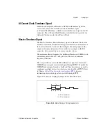
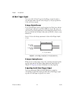
You can use a signal connected to any PFI or RTSI <0..6> pin as the source 
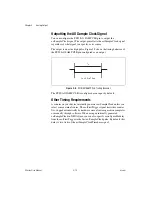
of ao/SampleClock. Figure 3-8 shows the timing requirements of the 
ao/SampleClock source.

Figure 3-8.  

ao/SampleClock Source Timing Requirements

Rising-Edge

Polarity

Falling-Edge

Polarity

t

w

t

w

 = 10 ns minimum

Summary of Contents for Data Acquisition Device E Series

Page 1: ...DAQ E Series E Series User Manual E Series User Manual February 2007 370503K 01...

Page 2: ...Lebanon 961 0 1 33 28 28 Malaysia 1800 887710 Mexico 01 800 010 0793 Netherlands 31 0 348 433 466 New Zealand 0800 553 322 Norway 47 0 66 90 76 60 Poland 48 22 3390150 Portugal 351 210 311 210 Russia...

Page 3: ...g storing in an information retrieval system or translating in whole or in part without the prior written consent of National Instruments Corporation National Instruments respects the intellectual pro...

Page 4: ...nt of Communications DOC Changes or modifications not expressly approved by NI could void the user s authority to operate the equipment under the FCC Rules Class A Federal Communications Commission Th...

Page 5: ...cumentation and Specifications xx Training Courses xx Technical Support on the Web xx Chapter 1 DAQ System Overview DAQ Hardware 1 2 DAQ STC 1 3 Calibration Circuitry 1 3 Internal or Self Calibration...

Page 6: ...nels 2 11 Minimize Voltage Step between Adjacent Channels 2 12 Avoid Scanning Faster than Necessary 2 12 Example 1 2 12 Example 2 2 13 AI Data Acquisition Methods 2 13 Software Timed Acquisitions 2 13...

Page 7: ...2 Using a Digital Source 2 33 Using an Analog Source 2 33 Outputting the AI Start Trigger Signal 2 33 AI Reference Trigger Signal 2 34 Using a Digital Source 2 35 Using an Analog Source 2 36 Outputtin...

Page 8: ...g Source 3 6 Outputting the AO Start Trigger Signal 3 6 AO Pause Trigger Signal 3 7 Using a Digital Source 3 7 Using an Analog Source 3 7 Connecting Analog Output Signals 3 8 Waveform Generation Timin...

Page 9: ...ting Started with DIO Applications in Software 4 10 Chapter 5 Counters Counter Triggering 5 1 Start Trigger 5 1 Pause Trigger 5 2 Counter Timing Signals 5 2 Counter 0 Source Signal 5 3 Counter 0 Gate...

Page 10: ...E and DAQPnP 9 1 Using PXI with CompactPCI 9 1 Data Transfer Methods 9 2 Direct Memory Access DMA 9 2 Interrupt Request IRQ 9 2 Programmed I O 9 2 Changing Data Transfer Methods between DMA and IRQ 9...

Page 11: ...Contents National Instruments Corporation xiii E Series User Manual Appendix B I O Connector Pinouts Appendix C Troubleshooting Appendix D Technical Support and Professional Services Glossary Index...

Page 12: ...options to a final action The sequence File Page Setup Options directs you to pull down the File menu select the Page Setup item and select Options from the last dialog box This icon denotes a note wh...

Page 13: ...stall your NI DAQmx supported DAQ device and how to confirm that your device is operating properly Select Start All Programs National Instruments NI DAQ DAQ Getting Started Guide The NI DAQ Readme lis...

Page 14: ...d by this version of NI DAQmx Base Select Start All Programs National Instruments NI DAQmx Base DAQmx Base Readme The NI DAQmx Base VI Reference Help contains VI reference and general information abou...

Page 15: ...ep instructions about creating a measurement task using the DAQ Assistant In LabWindows CVI select Help Contents then select Using LabWindows CVI Data Acquisition The NI DAQmx Library book of the LabW...

Page 16: ...Traditional NI DAQ Legacy Function Reference Help and NI DAQmx C Reference Help describe the C functions and attributes Select Start All Programs National Instruments NI DAQ and the document title for...

Page 17: ...e Device Document Browser device documents are accessible from Start All Programs National Instruments NI DAQ Browse Device Documentation Training Courses If you need more help getting started develop...

Page 18: ...hows a typical DAQ system setup which includes transducers signal conditioning cables that connect the various devices to the accessories the E Series device and the programming software Refer to the...

Page 19: ...ardware DAQ hardware digitizes signals performs D A conversions to generate analog output signals and measures and controls digital I O signals 1 Sensors and Transducers 2 Terminal Block Accessory 3 S...

Page 20: ...output Calibration Circuitry Calibration is the process of making adjustments to a measurement device to reduce errors associated with measurements Without calibration the measurement results of your...

Page 21: ...NI 6013 NI 6014 NI 6015 and NI 6016 using NI DAQmx refer to the E S M B Series Calibration Procedure for NI DAQmx For a detailed calibration procedure for B E Series devices using Traditional NI DAQ...

Page 22: ...lication software refer to Common Sensors in the NI DAQmx Help which you can access from Start All Programs National Instruments NI DAQ NI DAQmx Help or the LabVIEW 8 x Help Signal Conditioning Option...

Page 23: ...e portable Integrates well with other laptop computer measurement technologies High bandwidth Acquire signals at rates up to 1 25 MHz Connectivity Incorporates panelette technology to offer custom con...

Page 24: ...nnect an E Series device and an accessory 1 Select an E Series device 2 Using Table 1 1 or Table 1 2 as a guide determine which accessories are appropriate for that device Select an accessory Table 1...

Page 25: ...se accessories are used with the second 68 pin connector SH100100 shielded 100 pin E Series with 16 AI channels and 32 DIO lines NI PCI 6025E SH1006868 shielded splits into two 68 pin connectors these...

Page 26: ...nectors and a back shell kit for making custom 68 pin cables are available from NI For more information about the 68 and 100 pin BNC 2111 BNC accessory for 68 or 100 pin E Series devices BNC 2115 BNC...

Page 27: ...Getting Started Guide for more information about the two drivers Traditional NI DAQ Legacy and NI DAQmx each include a collection of programming examples to help you get started developing an applicat...

Page 28: ...e ended AI measurements in RSE mode and the bias current return point for DIFF measurements All three ground references AI GND AO GND and D GND are connected on the device AI 0 15 AI GND Input AI Chan...

Page 29: ...eripheral interface P3 7 is the MSB P3 0 is the LSB 5 V D GND Output 5 V Power Source These pins provide 5 V power AI HOLD COMP D GND Output AI Hold Complete Event Signal When enabled this signal puls...

Page 30: ...As an output this pin is the Ctr1Gate signal This signal reflects the actual gate signal connected to the general purpose Counter 1 CTR 1 OUT D GND Input CTR 1 OUT As an input this pin can be used to...

Page 31: ...ut PFI 9 As an input this pin is a PFI Output Counter 0 Gate Signal As an output this pin is the Ctr0Gate signal This signal reflects the actual gate signal connected to the general purpose Counter 0...

Page 32: ...0 DIOA DIOB DIOC P0 P1 P2 EXTREF AO EXT REF or EXT REF EXT_STROBE EXT STROBE EXT_TRIG EXT TRIG EXT_CONV EXT CONV FREQ_OUT FREQ OUT or F OUT GPCTR0_GATE CTR 0 GATE GPCTR0_OUT CTR 0 OUT GPCTR0_SOURCE CT...

Page 33: ...find your device power rating refer to the specifications document for your device Caution Never connect these 5 V power pins to analog or digital ground or to any other voltage source on the E Serie...

Page 34: ...d determine how you connect these AI signals to the E Series devices This chapter provides an overview of the different types of signal sources and AI configuration modes Analog Input Circuitry Mux Ea...

Page 35: ...digital number AI FIFO A large first in first out FIFO buffer holds data during A D conversions to ensure that no data is lost E Series devices can handle multiple A D conversion operations with DMA i...

Page 36: ...Choose an input range that matches the expected input range of your signal A large input range can accommodate a large signal variation but reduces the voltage resolution Choosing a smaller input rang...

Page 37: ...2 Input Ranges for NI 6011E and NI 6030E 6031E 6032E 6033E Input Range Gain Polarity Precision NI 6011E NI 6030E 6030E 6032E 6033E 0 to 10 V 0 to 5 V 0 to 2 V 0 to 1 V 0 to 500 mV 0 to 200 mV 0 to 10...

Page 38: ...ction for more information about using these input configurations Table 2 3 Input Ranges for NI 6023E 6024E 6025E and NI 6034E 6035E 6036E Input Range Gain Resolution NI 6023E 6024E 6025E NI 6034E 603...

Page 39: ...A in a different way The PGIA applies gain and common mode voltage rejection and presents high input impedance to the AI signals connected to the device Signals are routed to the positive and negative...

Page 40: ...mage resulting from such signal connections The maximum input voltage ratings are listed in the specifications document for each E Series family NI 6031E NI 6033E and NI 6071E Only For these extended...

Page 41: ...reading This process removes the effects of quantization and reduces measurement noise resulting in improved resolution For high speed applications not involving averaging or spectral analysis you may...

Page 42: ...I channel the device configures the NI PGIA with the input range of the new channel The NI PGIA then amplifies the input signal with the gain and polarity for the new input range Settling time refers...

Page 43: ...dances of 1 k The settling time specifications for your device assume a 1 k source Large source impedances increase the settling time of the PGIA and so decrease the accuracy at fast scanning rates Se...

Page 44: ...1 mV The approximately 4 V step from 4 V to 1 mV is 4 000 of the new full scale range For a 12 bit device to settle within 0 012 120 ppm or 1 2 LSB of the 100 mV full scale range on channel 1 the inpu...

Page 45: ...ry between 4 V and 0 V Scanning channels in the order 0 2 4 1 3 5 will produce more accurate results than scanning channels in the order 0 1 2 3 4 5 Avoid Scanning Faster than Necessary Designing your...

Page 46: ...ns hardware timed acquisitions can be buffered or non buffered Software Timed Acquisitions With a software timed acquisition software controls the rate of the acquisition Software sends a separate com...

Page 47: ...a samples and stopping a continuous acquisition continues until you stop the operation A continuous acquisition is also referred to as double buffered or circular buffered acquisition If data cannot b...

Page 48: ...rce specify a source and an edge The source can be an external signal connected to any PFI or RTSI 0 6 pin The source can also be one of several internal signals on your DAQ device Refer to Device Rou...

Page 49: ...he AI Reference Trigger Signal section for a complete description of the use of ai StartTrigger and ai ReferenceTrigger in a pretrigger DAQ operation AI Reference Trigger Signal You can use the AI Ref...

Page 50: ...tations before the DAQ device discards it Refer to the KnowledgeBase document Can a Pretriggered Acquisition be Continuous for more information When the reference trigger occurs the DAQ device continu...

Page 51: ...gger signal Figure 2 7 shows the timing requirements of the ai ReferenceTrigger source Figure 2 7 ai ReferenceTrigger Source Timing Requirements Using an Analog Source When you use an analog trigger s...

Page 52: ...rce can be an external signal connected to any PFI or RTSI 0 6 pin The source can also be one of several other internal signals on your DAQ device Refer to Device Routing in MAX in the NI DAQmx Help o...

Page 53: ...following sections discuss the types of signal sources specify the use of single ended and DIFF measurements and provide recommendations for measuring both floating and ground referenced signal source...

Page 54: ...ct To Building Ground Ground Referenced Signal Sources Examples Ungrounded thermocouples Signal conditioning with isolated outputs Battery devices Examples Plug in instruments with non isolated output...

Page 55: ...nt with respect to the device assuming that the computer is plugged into the same power system as the source Non isolated outputs of instruments and devices that plug into the building power system fa...

Page 56: ...noisy environments DIFF signal connections reduce noise pickup and increase common mode noise rejection DIFF signal connections also allow input signals to float within the common mode limits of the...

Page 57: ...l source and the device In addition with DIFF input connections the PGIA can reject common mode noise pickup in the leads connecting the signal sources to the device The PGIA can reject common mode si...

Page 58: ...rce impedance The resistor puts the signal path nearly in balance so that about the same amount of noise couples onto both connections yielding better rejection of electrostatically coupled noise This...

Page 59: ...se the device provides the reference ground point for the external signal NRSE input mode is used for ground referenced signal sources in this case the external signal supplies its own reference groun...

Page 60: ...input of the PGIA and connect the signal local ground reference to the negative input of the PGIA The ground point of the signal therefore connects to the AI SENSE pin as shown in Figure 2 12 Any pot...

Page 61: ...ect common mode noise Use individually shielded twisted pair wires to connect AI signals to the device With this type of wire the signals attached to the positive and negative input channels are twist...

Page 62: ...rol of the AI Config VI This input has a one to one correspondence with the channels control of the VI You must list all channels either individually or in groups of channels with the same input confi...

Page 63: ...ng engine Figure 2 15 Analog Input Timing Engine Clock Routing and Timing Options E Series devices use the ai SampleClock and ai ConvertClock signals to perform interval sampling As Figure 2 16 shows...

Page 64: ...r example if an E Series device has a sampling rate of 200 kS s this sampling rate is aggregate one channel at 200 kS s or two channels at 100 kS s per channel illustrates the relationship An acquisit...

Page 65: ...cquisition If an ai ReferenceTrigger pulse occurs before the specified number of pretrigger samples are acquired the trigger pulse is ignored Otherwise when the ai ReferenceTrigger pulse occurs the sa...

Page 66: ...rising edge or falling edge of the ai StartTrigger signal Figure 2 19 shows the timing requirements of the ai StartTrigger source Figure 2 19 ai StartTrigger Timing Requirements Using an Analog Sourc...

Page 67: ...isition In Traditional NI DAQ Legacy a reference trigger is referred to as a stop trigger To use a reference trigger specify a buffer of finite size and a number of pretrigger samples samples that occ...

Page 68: ...can be an external signal connected to any PFI or RTSI 0 6 pin The source can also be one of several internal signals on your DAQ device Refer to Device Routing in MAX in the NI DAQmx Help or the LabV...

Page 69: ...f the PFI 1 AI REF TRIG pin configured as an output Figure 2 23 PFI 1 AI REF TRIG Timing Behavior The PFI 1 AI REF TRIG pin is configured as an input by default AI Pause Trigger Signal You can use the...

Page 70: ...ist once for every ai SampleClock A measurement acquisition consists of one or more samples The source of the ai SampleClock signal can be internal or external You specify whether the measurement samp...

Page 71: ...ior your DAQ device briefly pulses the PFI 7 AI SAMP CLK pin once for every occurrence of ai SampleClock With level behavior your DAQ device drives PFI 7 AI SAMP CLK high during the entire sample The...

Page 72: ...lso specify a configurable delay from the ai StartTrigger to the first ai SampleClock pulse By default this delay is two ticks of the ai SampleClockTimebase signal When using an externally generated a...

Page 73: ...Onboard Clock source for the ai SampleClock You can configure the polarity selection for ai SampleClockTimebase as either rising or falling edge The maximum allowed frequency is 20 MHz with a minimum...

Page 74: ...stest conversion rate possible for the device with 10 s of delay added between each conversion to allow the channel to some time settle Caution Setting the conversion rate higher than the maximum rate...

Page 75: ...utting the AI Convert Clock Signal You can configure the PFI 2 AI CONV CLK pin to output the ai ConvertClock signal The output pin reflects the ai ConvertClock signal regardless of what signal you spe...

Page 76: ...nless the proper timing requirements are met For example the device ignores both the ai SampleClock and ai ConvertClock until it receives a valid ai StartTrigger signal Once the device recognizes an a...

Page 77: ...st for Convert Clock Sample Clock pulses are gated off ai ConvertClock ai SampleClock 1 2 3 Convert Clock too fast for Sample Clock Convert Clock pulses are gated off ai ConvertClock ai SampleClock 1...

Page 78: ...g input analog output and counter subsystems It is available as an output on the I O connector but you must use one or more counters to do so The maximum allowed frequency for the MasterTimebase is 20...

Page 79: ...Figure 2 34 ai HoldCompleteEvent Timing External Strobe Signal External Strobe is an output only signal on the EXT STROBE pin that generates either a single pulse or a sequence of eight pulses in the...

Page 80: ...applications Single Point Analog Input Finite Analog Input Continuous Analog Input You can perform these applications through DMA interrupt or programmed I O data transfer mechanisms Some of the appli...

Page 81: ...m generation Refer to Appendix A Device Specific Information for specific information about the capabilities of your device Analog Output Circuitry DACs Digital to analog converters DACs convert digit...

Page 82: ...ices such as the NI 6013 6014 and NI 6015 6016 are bipolar only with an internal reference Refer to the specifications document for your device for more information about range setting options Referen...

Page 83: ...values written to the AO channel range must be positive Reglitch Selection NI 6052E and NI 6070E 6071E Devices Only In normal operation a DAC output glitches whenever it is updated with a new value Th...

Page 84: ...signal controls the rate of the generation This signal can be generated internally on your device or provided externally Hardware timed generations have several advantages over software timed generati...

Page 85: ...m there Once the data is downloaded new data cannot be written to the FIFO To use FIFO regeneration the entire buffer must fit within the FIFO size The advantage of using FIFO regeneration is that it...

Page 86: ...mx Help or the LabVIEW 8 x Help for more information Figure 3 2 shows the timing requirements of the ao StartTrigger digital source Figure 3 2 ao StartTrigger Digital Source Timing Requirements Using...

Page 87: ...se does not take effect until the beginning of the next sample This signal is not available as an output Using a Digital Source To use ao PauseTrigger specify a source and a polarity The source can be...

Page 88: ...nnel 1 AO GND is the ground reference signal for both AO channels and the external reference signal Figure 3 4 shows how to make AO connections to the device Figure 3 4 Analog Output Connections Note...

Page 89: ...ftware command Using a Digital Source To use ao StartTrigger specify a source and an edge The source can be an external signal connected to any PFI or RTSI 0 6 pin The source can also be one of severa...

Page 90: ...ing Behavior The PFI 6 AO START TRIG pin is configured as an input by default AO Pause Trigger Signal You can use the AO Pause trigger signal ao PauseTrigger to mask off samples in a DAQ sequence That...

Page 91: ...or external You can specify whether the DAC update begins on the rising edge or falling edge of the ao SampleClock signal Using an Internal Source By default ao SampleClock is created internally by d...

Page 92: ...AO SAMP CLK Timing Behavior The PFI 5 AO SAMP CLK is configured as an input by default Other Timing Requirements A counter on your device internally generates ao SampleClock unless you select some ex...

Page 93: ...SampleClockTimebase is divided down to provide the Onboard Clock source for the ao SampleClock You specify whether the samples begin on the rising or falling edge of ao SampleClockTimebase You might...

Page 94: ...on the board are derived It controls the timing for the analog input analog output and counter subsystems It is available as an output on the I O connector but you must use one or more counters to do...

Page 95: ...following analog output applications Single Point Generation Finite Generation Continuous Generation Waveform Generation You can perform these generations through DMA interrupt or programmed I O data...

Page 96: ...rcuitry of the E Series device Figure 4 1 DIO Circuitry Block Diagram E Series devices contain eight lines of DIO P0 0 7 for general purpose use You can individually configure each line with software...

Page 97: ...de 0 strobed I O mode 1 and bidirectional I O mode 2 In modes 1 and 2 the three ports are divided into two groups group A and group B Each group has eight data bits plus control and status bits from P...

Page 98: ...value on the line is 0 4 VDC The DIO lines provide a maximum of 2 5 mA at 3 7 V in the high state Using the largest possible resistor ensures that you do not use more current than necessary to perfor...

Page 99: ...where V 0 4 V Voltage across RL I 46 A 4 6 V across the 100 k pull up resistor 10 A 10 A maximum leakage current Therefore RL 7 1 k 0 4 V 56 A This resistor value 7 1 k provides a maximum of 0 4 V on...

Page 100: ...ice indicating that it has received the data from your DIO device OBF Output Output buffer full A low signal on this handshaking line indicates that data has been written to the port INTR Output Inter...

Page 101: ...ransfer in mode 1 Figure 4 3 Input Transfer in Mode 1 Timing Specifications Table 4 3 Input Transfer in Mode 1 Timing Specifications Name Description Minimum ns Maximum ns T1 STB Pulse Width 100 T2 ST...

Page 102: ...output transfer in mode 1 Figure 4 4 Output Transfer in Mode 1 Timing Specifications Table 4 4 Output Transfer in Mode 1 Timing Specifications Name Description Minimum ns Maximum ns T1 WR 0 to INTR 0...

Page 103: ...onal Transfer Timing Specifications Table 4 5 Bidirectional Transfer Timing Specification Name Description Minimum ns Maximum ns T1 WR 1 to OBF 0 150 T2 Data before STB 1 20 T3 STB Pulse Width 100 T4...

Page 104: ...sistor This pull up resistor sets the P0 0 pin to a logic high when the output is in a high impedance state Caution If you enable a PFI line for output do not connect any external signal source to it...

Page 105: ...nd the computer NI is not liable for any damage resulting from such signal connections Getting Started with DIO Applications in Software You can use the E Series device in the following digital I O ap...

Page 106: ...can directly initiate these actions An analog trigger can indirectly initiate these actions by routing the Analog Comparison Event from a triggered analog input or output task to the counter as a dig...

Page 107: ...sing edge of the source signal This timing diagram assumes that the counters are programmed to count rising edges The same timing diagram but with the source signal inverted and referenced to the fall...

Page 108: ...nal state changes occur within 80 ns after the rising or falling edge of the source signal For information about the internal routing available on the DAQ STC counter timers refer to Counter Parts in...

Page 109: ...al The Ctr0Gate signal is configured in edge detection or level detection mode depending on the application performed by the counter The gate signal can perform many different operations including sta...

Page 110: ...pulse generation mode the counter drives Ctr0InternalOutput with the generated pulses To enable this behavior software configures the counter to toggle Ctr0InternalOutput on TC Ctr0InternalOutput can...

Page 111: ...ng an external signal to control the count direction do not use the P0 6 pin for output If you do not enable externally controlled count direction the P0 6 pin is free for general use Counter 1 Source...

Page 112: ...urce signal Counter 1 Gate Signal You can select any PFI as well as many other internal signals like the Counter 1 Gate Ctr1Gate signal The Ctr1Gate signal is configured in edge detection or level det...

Page 113: ...software selectable for both options Figure 5 9 shows the behavior of the Ctr1InternalOutput signal Figure 5 9 Ctr1InternalOutput Signal Behavior You can use Ctr1InternalOutput in the following appli...

Page 114: ...rs one through 16 The input clock of the frequency generator is software selectable from the internal 10 MHz and 100 kHz timebases The output polarity is software selectable This output is set to high...

Page 115: ...ency Measurement Period Measurement Pulse Width Measurement Semi Period Measurement Pulse Generation You can perform these measurements through DMA interrupt or programmed I O data transfer mechanisms...

Page 116: ...ection for any of the timing signals but the edge or level detection depends upon the particular timing signal being controlled The detection requirements for each timing signal are listed within the...

Page 117: ...be output on PFI pins AI Start Trigger Signal AI Reference Trigger Signal AI Sample Clock Signal AI Convert Clock Signal AO Start Trigger Signal AO Sample Clock Signal Counter 0 Source Signal Counter...

Page 118: ...ed description of which routes are possible on your device in Measurement Automation Explorer MAX select Devices and Interfaces your device then select the Device Routes tab Timing Signal Routing The...

Page 119: ...Counter 0 Gate Signal Counter 0 Up Down Signal Counter 1 Source Signal Counter 1 Gate Signal Counter 1 Up Down Signal Master Timebase Signal You also can control these timing signals by signals gener...

Page 120: ...and PFI 0 9 and the internal signals Onboard Clock and Ctr0InternalOutput On PCI and PXI devices many of these timing signals are also available as outputs on the PFI pins Note The Master Timebase si...

Page 121: ...the device These lines serve as connections to virtually all internal timing signals These PFIs are bidirectional As outputs they are not programmable and reflect the state of many analog input wavef...

Page 122: ...tion about routing signals in software refer to the NI DAQmx Help or the LabVIEW 8 x Help Table 7 1 Functions For Routing Signals Language Program Function LabVIEW NI DAQmx DAQmx Export Signal vi and...

Page 123: ...e RTSI bus interface and the PXI trigger signals on the PXI backplane This bus can route timing and trigger signals between several functions on as many as seven DAQ devices in the system Refer to the...

Page 124: ...Devices The RTSI trigger lines connect to other devices through the PXI bus on the PXI backplane RTSI 0 5 connect to PXI Trigger 0 5 respectively This signal connection scheme is shown in Figure 8 2...

Page 125: ...ng for a description of the signals shown in Figure 8 2 Note In NI DAQmx you can indirectly route timing signals not shown in the above diagrams to RTSI For a detailed description of which routes are...

Page 126: ...ive this timebase signal The default configuration at startup is to use the internal timebase without driving the RTSI bus timebase signal Note DAQCard and DAQPad devices do not interface to the RTSI...

Page 127: ...se address of the device The MITE implements the PCI Local Bus Specification so that the interrupts and base memory addresses are all software configured Using PXI with CompactPCI Using PXI compatible...

Page 128: ...mmed I O Direct Memory Access DMA DMA is a method to transfer data between the device and computer memory without the involvement of the CPU This method makes DMA the fastest available data transfer m...

Page 129: ...your device Each operation for example AI AO and so on that requires a DMA channel uses that method until all of the DMA channels are used Once all of the DMA channels are used you will get an error...

Page 130: ...ffect the following Analog input acquisitions Analog output generation Counter behavior Note Not all E Series devices support analog triggering Refer to Appendix A Device Specific Information for info...

Page 131: ...E Series devices can generate a trigger on an analog signal Figure 10 2 shows the analog trigger circuit Figure 10 2 Analog Trigger Circuit You must specify a source and an analog trigger type The so...

Page 132: ...should not route different AI channels to the PGIA If a different channel is routed to the PGIA the trigger condition on the desired channel could be missed The other channels could also generate fal...

Page 133: ...try to detect when the analog signal is below or above a level you specify In below level analog triggering mode the trigger is generated when the signal value is less than Level as shown in Figure 10...

Page 134: ...the signal crosses below Level minus hysteresis as shown in Figure 10 5 Figure 10 5 High Hysteresis When using Hysteresis with a falling slope the trigger asserts when the signal starts above Level an...

Page 135: ...el the PGIA amplifies the AI channel signal before driving the analog trigger circuitry If you configure the AI channel to have a small input range you can trigger on very small voltage changes in the...

Page 136: ...62E NI 6070E 6071E Family Note To obtain documentation for devices not listed here refer to ni com manuals NI 6011E NI PCI MIO 16XE 50 The NI 6011E NI PCI MIO 16XE 50 is a Plug and Play multifunction...

Page 137: ...50 Block Diagram PCI Bus Configuration Memory Timing PFI Trigger I O Connector 2 Digital I O 8 16 Bit Sampling A D Converter Programmable Gain Amplifier Calibration Mux Mux Mode Selection Switches Vol...

Page 138: ...ications for more detailed information on the device NI 6011E NI PCI MIO 16XE 50 Pinout Figure A 2 shows the NI 6011E NI PCI MIO 16XE 50 device pinout Note Some hardware accessories may not yet reflec...

Page 139: ...5 V D GND P0 6 P0 1 D GND P0 4 AO EXT REF AO 1 AO 0 AI 15 AI GND AI 6 AI 13 AI GND AI 4 AI GND AI 3 AI 10 AI GND AI 1 AI 8 D GND PFI 8 CTR 0 SRC PFI 7 AI SAMP CLK CTR 1 OUT PFI 4 CTR 1 GATE PFI 3 CTR...

Page 140: ...annels eight differential with 16 bit resolution Eight lines of TTL compatible DIO Two 24 bit counter timers for TIO A 68 pin I O connector The NI 6014 features the following 16 AI channels eight diff...

Page 141: ...5 Terminal Name Equivalents for the Traditional NI DAQ Legacy signal names Analog Mode Multiplexer Timing PFI Trigger I O Connector Digital I O A D Converter EEPROM EEPROM PGIA Voltage REF Calibration...

Page 142: ...ND 5 V D GND P0 6 P0 1 D GND P0 4 NC NC NC AI 15 AI GND AI 6 AI 13 AI GND AI 4 AI GND AI 3 AI 10 AI GND AI 1 AI 8 D GND PFI 8 CTR 0 SRC PFI 7 AI SAMP CLK CTR 1 OUT PFI 4 CTR 1 GATE PFI 3 CTR 1 SRC PFI...

Page 143: ...out Figure A 5 shows the NI 6014 device pinout Note Some hardware accessories may not yet reflect the NI DAQmx terminal names If you are using an E Series device in Traditional NI DAQ Legacy refer to...

Page 144: ...5 V D GND P0 6 P0 1 D GND P0 4 NC AO 1 AO 0 AI 15 AI GND AI 6 AI 13 AI GND AI 4 AI GND AI 3 AI 10 AI GND AI 1 AI 8 D GND PFI 8 CTR 0 SRC PFI 7 AI SAMP CLK CTR 1 OUT PFI 4 CTR 1 GATE PFI 3 CTR 1 SRC P...

Page 145: ...res the following 16 AI channels eight differential with 16 bit resolution Two AO channels with 16 bit resolution DAQPad 6015 Eight lines of TTL compatible DIO DAQPad 6016 32 lines of TTL compatible D...

Page 146: ...rminals Prototyping areas 8 0 in 6 75 in 1 4 in Stackable Integrated strain relief A removable lid DAQPad 6015 BNC Eight AI BNCs Two AO BNCs Four digital BNCs A spring loaded Combicon connector for ot...

Page 147: ...log Input Timing Control Analog Output Timing Control Digital I O Trigger Interface Counter Timing I O RTSI Bus Interface DMA Interrupt Request Bus Interface 8 8 AI Control IRQ DMA AO Control Data 16...

Page 148: ...onsiderations To measure a floating signal source move the switch to the FS position To measure a ground referenced signal source move the switch to the GS position Figure A 7 shows the source type sw...

Page 149: ...Ended Connections When you set the source type to the GS position and software configure the device for single ended input each BNC connector provides access to two single ended channels AI x and AI...

Page 150: ...s Figure A 10 BNC DAQPads Analog Output Circuitry Refer to the Connecting Analog Output Signals section of Chapter 3 Analog Output for more information Counter 0 Out and PFI 0 AI Start Trigger You can...

Page 151: ...is internally connected to pin 22 on the 30 pin I O connector Figure A 13 shows the connection of the User 1 2 BNCs Figure A 13 User 1 2 BNC Connection Figure A 14 shows another example of how to use...

Page 152: ...ll screwdriver to press down the orange spring release button at a terminal and insert a wire Releasing the orange spring release button will lock the wire securely in place You can remove the Combico...

Page 153: ...Y DAQPad 6015 6016 State Off Off The device is not powered Off On The device is configured but there is no activity over the bus On On The device is configured and there is activity over the bus Blink...

Page 154: ...gure A 16 The fuse is located between the power connector and switch near the back of the device Figure A 16 DAQPad 6015 6016 Fuse Removal To remove the fuse from the DAQPad 6015 BNC or mass terminati...

Page 155: ...Information E Series User Manual A 20 ni com Figure A 17 DAQPad 6015 Mass Termination Device DAQPad 6015 6016 Specifications Refer to the NI DAQPad 6015 6016 Family Specifications for more detailed i...

Page 156: ...AQ System Overview P0 0 33 49 CTR 0 OUT P0 1 34 50 PFI 8 CTR 0 SOURCE D GND 35 51 D GND P0 2 36 52 PFI 9 CTR 0 GATE P0 3 37 53 PFI 5 AO SAMP CLK P0 4 38 54 PFI 6 AO START TRIG D GND 39 55 D GND P0 5 4...

Page 157: ...O Connector Signal Descriptions section of Chapter 1 DAQ System Overview NI DAQPad 6015 Mass Termination Pinout Figure A 20 shows the NI DAQPad 6015 mass termination device pinout Note Some hardware...

Page 158: ...G D GND D GND 5 V D GND P0 6 P0 1 D GND P0 4 NC AO 1 AO 0 AI 15 AI GND AI 6 AI 13 AI GND AI 4 AI GND AI 3 AI 10 AI GND AI 1 AI 8 D GND PFI 8 CTR 0 SRC PFI 7 AI SAMP CLK CTR 1 OUT PFI 4 CTR 1 GATE PFI...

Page 159: ...NI DAQ Legacy signal names Figure A 21 NI DAQPad 6016 Pinout For a detailed description of each signal refer to the I O Connector Signal Descriptions section of Chapter 1 DAQ System Overview NI 6020E...

Page 160: ...fering different I O connectivity and form factors These versions are illustrated in Table A 3 Note The DAQPad 6020E devices are compatible with Traditional NI DAQ Legacy only Table A 3 DAQPad 6020E V...

Page 161: ...ation To measure a floating signal source move the switch to the FS position To measure a ground referenced signal source move the switch to the GS Timing PFI Trigger I O Connector 4 USB Connector Ext...

Page 162: ...on AI x is grounded through a 0 1 F capacitor in parallel with a 5 k resistor Figure A 24 BNC DAQPads Analog Input Circuitry FS GS FS GS FS GS FS GS FS GS FS GS FS GS FS GS 1 3 5 7 9 11 13 15 17 19 21...

Page 163: ...ngle ended input each BNC connector provides access to two single ended channels AI x and AI x 8 For example the BNC connector labeled AI 0 provides access to single ended channels AI 0 and AI 8 the B...

Page 164: ...s Figure A 27 shows circuitry of the AO EXT REF on BNC DAQPads Figure A 27 AO EXT REF Refer to the Reference Selection section of Chapter 3 Analog Output for more information Counter 0 Out and PFI 0 A...

Page 165: ...is internally connected to pin 22 on the 30 pin I O connector Figure A 30 shows the connection of the User 1 2 BNCs Figure A 30 BNC User 1 2 Connection Figure A 31 shows another example of how to use...

Page 166: ...crewdriver to press down the orange spring release button at a terminal and insert a wire Releasing the orange spring release button will lock the wire securely in place You can remove the Combicon pl...

Page 167: ...names If you are using an E Series device in Traditional NI DAQ Legacy refer to Table 1 5 Terminal Name Equivalents for the Traditional NI DAQ Legacy signal names Table A 4 DAQPad 6020E LEDs LED DAQP...

Page 168: ...ND D GND 5 V D GND P0 6 P0 1 D GND P0 4 AO EXT REF AO 1 AO 0 AI 15 AI GND AI 6 AI 13 AI GND AI 4 AI GND AI 3 AI 10 AI GND AI 1 AI 8 D GND PFI 8 CTR 0 SRC PFI 7 AI SAMP CLK CTR 1 OUT PFI 4 CTR 1 GATE P...

Page 169: ...Terminal Name Equivalents for the Traditional NI DAQ Legacy signal names Figure A 34 NI DAQPad 6020E BNC Pinout For a detailed description of each signal refer to the I O Connector Signal Description...

Page 170: ...IO A 68 pin I O connector The NI 6024E features the following 16 AI channels eight differential with 12 bit resolution Two AO channels with 12 bit resolution Eight lines of TTL compatible DIO Two 24 b...

Page 171: ...cuitry Analog Mode Multiplexer Voltage REF Calibration DACs Calibration DACs DAC0 DAC1 DAQ STC Analog Input Timing Control Analog Output Timing Control Digital I O Trigger Counter Timing I O RTSI Bus...

Page 172: ...ditional NI DAQ Legacy refer to Table 1 5 Terminal Name Equivalents for the Traditional NI DAQ Legacy signal names 3 PCMCIA Connector 12 Bit Sampling A D Converter NI PGIA Gain Amplifier Calibration M...

Page 173: ...P0 6 P0 1 D GND P0 4 NC NC NC AI 15 AI GND AI 6 AI 13 AI GND AI 4 AI GND AI 3 AI 10 AI GND AI 1 AI 8 D GND PFI 8 CTR 0 SRC PFI 7 AI SAMP CLK CTR 1 OUT PFI 4 CTR 1 GATE PFI 3 CTR 1 SRC PFI 2 AI CONV C...

Page 174: ...NI 6024E Pinout Figure A 38 shows the NI 6024E device pinout Note Some hardware accessories may not yet reflect the NI DAQmx terminal names If you are using an E Series device in Traditional NI DAQ L...

Page 175: ...0 6 P0 1 D GND P0 4 NC AO 1 AO 0 AI 15 AI GND AI 6 AI 13 AI GND AI 4 AI GND AI 3 AI 10 AI GND AI 1 AI 8 D GND PFI 8 CTR 0 SRC PFI 7 AI SAMP CLK CTR 1 OUT PFI 4 CTR 1 GATE PFI 3 CTR 1 SRC PFI 2 AI CONV...

Page 176: ...NI 6025E Pinout Figure A 39 shows the NI 6025E device pinout Note Some hardware accessories may not yet reflect the NI DAQmx terminal names If you are using an E Series device in Traditional NI DAQ L...

Page 177: ...AI SAMP CLK PFI 6 AO START TRIG PFI 5 AO SAMP CLK CTR 1 OUT PFI 4 CTR 1 GATE PFI 3 CTR 1 SRC PFI 2 AI CONV CLK PFI 1 AI REF TRIG PFI 0 AI START TRIG EXT STROBE AI HOLD COMP 5 V 5 V D GND P0 7 P0 3 P0...

Page 178: ...pin I O connector The NI 6031E features the following 64 AI channels 32 differential with 16 bit resolution Two AO channels with 16 bit resolution Eight lines of TTL compatible DIO Two 24 bit counter...

Page 179: ...Trigger I O Connector 3 2 2 Digital I O 8 12 Bit Sampling A D Converter REF Buffer Programmable Gain Amplifier Calibration Mux Mux Mode Selection Switches Voltage REF Calibration DACs 4 Calibration DA...

Page 180: ...Name Equivalents for the Traditional NI DAQ Legacy signal names PCI Bus Configuration Memory Timing PFI Trigger I O Connector 3 2 2 RTSI Bus Digital I O 8 16 Bit Sampling A D Converter NI PGIA Gain A...

Page 181: ...D P0 6 P0 1 D GND P0 4 AO EXT REF AO 1 AO 0 AI 15 AI GND AI 6 AI 13 AI GND AI 4 AI GND AI 3 AI 10 AI GND AI 1 AI 8 D GND PFI 8 CTR 0 SRC PFI 7 AI SAMP CLK CTR 1 OUT PFI 4 CTR 1 GATE PFI 3 CTR 1 SRC PF...

Page 182: ...0 NI 6030E Pinout Figure A 43 shows the PCI MIO 16XE 10 NI 6030E device pinout Note Some hardware accessories may not yet reflect the NI DAQmx terminal names If you are using an E Series device in Tra...

Page 183: ...D 5 V D GND P0 6 P0 1 D GND P0 4 AO EXT REF AO 1 AO 0 AI 15 AI GND AI 6 AI 13 AI GND AI 4 AI GND AI 3 AI 10 AI GND AI 1 AI 8 D GND PFI 8 CTR 0 SRC PFI 7 AI SAMP CLK CTR 1 OUT PFI 4 CTR 1 GATE PFI 3 CT...

Page 184: ...NI 6031E Pinout Figure A 44 shows the NI 6031E device pinout Note Some hardware accessories may not yet reflect the NI DAQmx terminal names If you are using an E Series device in Traditional NI DAQ L...

Page 185: ...R 1 SRC PFI 2 AI CONV CLK PFI 1 AI REF TRIG AI HOLD COMP 5 V 5 V D GND P0 7 P0 3 P0 6 P0 2 P0 5 P0 1 P0 4 P0 0 D GND AI SENSE AI 15 AI 7 AI 14 AI 6 AI 13 AI 5 AI 12 AI 4 AI 11 AI 3 AI 10 AI 2 AI 9 AI...

Page 186: ...ctor Signal Descriptions section of Chapter 1 DAQ System Overview NI 6032E Pinout Figure A 45 shows the NI 6032E device pinout Note Some hardware accessories may not yet reflect the NI DAQmx terminal...

Page 187: ...P0 6 P0 1 D GND P0 4 NC NC NC AI 15 AI GND AI 6 AI 13 AI GND AI 4 AI GND AI 3 AI 10 AI GND AI 1 AI 8 D GND PFI 8 CTR 0 SRC PFI 7 AI SAMP CLK CTR 1 OUT PFI 4 CTR 1 GATE PFI 3 CTR 1 SRC PFI 2 AI CONV C...

Page 188: ...NI 6033E Pinout Figure A 46 shows the NI 6033E device pinout Note Some hardware accessories may not yet reflect the NI DAQmx terminal names If you are using an E Series device in Traditional NI DAQ L...

Page 189: ...I 6 AO START TRIG PFI 5 AO SAMP CLK CTR 1 OUT PFI 4 CTR 1 GATE PFI 3 CTR 1 SRC PFI 2 AI CONV CLK PFI 1 AI REF TRIG PFI 0 AI START TRIG EXT STROBE AI HOLD COMP 5 V 5 V D GND P0 7 P0 3 P0 6 P0 2 P0 5 P0...

Page 190: ...rential with 16 bit resolution Two AO channels with 12 bit resolution Eight lines of TTL compatible DIO Two 24 bit counter timers for TIO A 68 pin I O connector The NI 6036E features the following 16...

Page 191: ...put Muxes Voltage REF Calibration DACs Calibration DACs DAC0 DAC1 No AO on NI 6034E DAQ STC Analog Input Timing Control Analog Output Timing Control Digital I O Trigger Interface Counter Timing I O RT...

Page 192: ...s device in Traditional NI DAQ Legacy refer to Table 1 5 Terminal Name Equivalents for the Traditional NI DAQ Legacy signal names I O Connector 3 PCMCIA Connector 16 Bit Sampling A D Converter NI PGIA...

Page 193: ...0 6 P0 1 D GND P0 4 NC NC NC AI 15 AI GND AI 6 AI 13 AI GND AI 4 AI GND AI 3 AI 10 AI GND AI 1 AI 8 D GND PFI 8 CTR 0 SRC PFI 7 AI SAMP CLK CTR 1 OUT PFI 4 CTR 1 GATE PFI 3 CTR 1 SRC PFI 2 AI CONV CLK...

Page 194: ...NI 6035E Pinout Figure A 50 shows the NI 6035E device pinout Note Some hardware accessories may not yet reflect the NI DAQmx terminal names If you are using an E Series device in Traditional NI DAQ L...

Page 195: ...0 6 P0 1 D GND P0 4 NC AO 1 AO 0 AI 15 AI GND AI 6 AI 13 AI GND AI 4 AI GND AI 3 AI 10 AI GND AI 1 AI 8 D GND PFI 8 CTR 0 SRC PFI 7 AI SAMP CLK CTR 1 OUT PFI 4 CTR 1 GATE PFI 3 CTR 1 SRC PFI 2 AI CONV...

Page 196: ...NI 6036E Pinout Figure A 51 shows the NI 6036E device pinout Note Some hardware accessories may not yet reflect the NI DAQmx terminal names If you are using an E Series device in Traditional NI DAQ L...

Page 197: ...P0 6 P0 1 D GND P0 4 NC AO 1 AO 0 AI 15 AI GND AI 6 AI 13 AI GND AI 4 AI GND AI 3 AI 10 AI GND AI 1 AI 8 D GND PFI 8 CTR 0 SRC PFI 7 AI SAMP CLK CTR 1 OUT PFI 4 CTR 1 GATE PFI 3 CTR 1 SRC PFI 2 AI CON...

Page 198: ...tures the following 16 AI channels eight differential with 12 bit resolution Two AO channels with 12 bit resolution Eight lines of TTL compatible DIO Two 24 bit counter timers for TIO A 68 pin I O con...

Page 199: ...A D Converter EEPROM NI PGIA Gain Amplifier Voltage REF Calibration DACs DAC0 DAC1 DAQ STC Trigger 8 8 AI Control Address Data Control Analog Input Control EEPROM Control MIO Interface MINI MITE Gener...

Page 200: ...GND 5 V D GND P0 6 P0 1 D GND P0 4 AO EXT REF AO 1 AO 0 AI 15 AI GND AI 6 AI 13 AI GND AI 4 AI GND AI 3 AI 10 AI GND AI 1 AI 8 D GND PFI 8 CTR 0 SRC PFI 7 AI SAMP CLK CTR 1 OUT PFI 4 CTR 1 GATE PFI 3...

Page 201: ...us computers The PCI MIO 16E 4 features the following 16 AI channels eight differential with 16 bit resolution Two AO channels with 12 bit resolution Eight lines of TTL compatible DIO Two 24 bit count...

Page 202: ...ation Memory Timing PFI Trigger I O Connector 3 2 Digital I O 8 12 Bit Sampling A D Converter NI PGIA Gain Amplifier Calibration Mux Mux Mode Selection Switches Voltage REF Calibration DACs 6 Calibrat...

Page 203: ...5 V D GND P0 6 P0 1 D GND P0 4 AO EXT REF AO 1 AO 0 AI 15 AI GND AI 6 AI 13 AI GND AI 4 AI GND AI 3 AI 10 AI GND AI 1 AI 8 D GND PFI 8 CTR 0 SRC PFI 7 AI SAMP CLK CTR 1 OUT PFI 4 CTR 1 GATE PFI 3 CTR...

Page 204: ...formance switchless jumperless hot pluggable DAQ device The 1394 interface automatically handles the assignment of all host resources and allows you to install the device without powering off the comp...

Page 205: ...es the different I O connectivity and form factors of each version Table A 5 NI DAQPad 6052E Versions Model I O Connector Form Factor DAQPad 6052E 68 pin SCSI II male Full size box 12 1 in 10 in 1 7 i...

Page 206: ...onverter REF Buffer Programmable Gain Amplifier Calibration Mux Mux Mode Selection Switches Voltage REF Calibration DACs 8 Calibration DACs DAC0 DAC1 DAQ STC Analog Input Timing Control Analog Output...

Page 207: ...ition Figure A 57 shows the source type switch locations on the front panel of the BNC DAQPads Figure A 57 BNC DAQPad Front Panel Figure A 58 shows the analog input circuitry on BNC DAQPads When the s...

Page 208: ...for single ended input each BNC connector provides access to two single ended channels AI x and AI x 8 For example the BNC connector labeled AI 0 provides access to single ended channels AI 0 and AI 8...

Page 209: ...Counter 0 Out and PFI 0 AI Start Trigger You can access the Counter 0 Out and PFI 0 AI Start Trigger signals through their respective pins on BNC DAQPads as shown in Figure A 62 and Figure A 63 Refer...

Page 210: ...and the USER 2 BNC is internally connected to pin 22 on the 30 pin I O connector Figure A 64 shows the connection of the User 1 2 BNCs Figure A 64 User 1 2 BNCs Figure A 65 shows another example of ho...

Page 211: ...river to press down the orange spring release button at a terminal and insert a wire Releasing the orange spring release button will lock the wire securely in place You can remove the Combicon plugs t...

Page 212: ...t Note Some hardware accessories may not yet reflect the NI DAQmx terminal names If you are using an E Series device in Traditional NI DAQ Legacy refer to Table 1 5 in Chapter 1 for the Traditional NI...

Page 213: ...D GND P0 6 P0 1 D GND P0 4 AO EXT REF AO 1 AO 0 AI 15 AI GND AI 6 AI 13 AI GND AI 4 AI GND AI 3 AI 10 AI GND AI 1 AI 8 D GND PFI 8 CTR 0 SRC PFI 7 AI SAMP CLK CTR 1 OUT PFI 4 CTR 1 GATE PFI 3 CTR 1 SR...

Page 214: ...detailed description of each signal refer to the I O Connector Signal Descriptions section of Chapter 1 DAQ System Overview NI PCI PXI 6052E The NI PCI PXI 6052E are Plug and Play multifunction AI AO...

Page 215: ...5 in Chapter 1 for the Traditional NI DAQ Legacy signal names PCI PXI Bus Configuration Memory Timing PFI Trigger I O Connector 6 2 2 RTSI Bus Digital I O 8 16 Bit Sampling A D Converter REF Buffer Pr...

Page 216: ...ND D GND 5 V D GND P0 6 P0 1 D GND P0 4 AO EXT REF AO 1 AO 0 AI 15 AI GND AI 6 AI 13 AI GND AI 4 AI GND AI 3 AI 10 AI GND AI 1 AI 8 D GND PFI 8 CTR 0 SRC PFI 7 AI SAMP CLK CTR 1 OUT PFI 4 CTR 1 GATE P...

Page 217: ...AI AO DIO and TIO DAQ device for computers equipped with Type II PCMCIA slots The DAQCard 6062E features the following 16 AI channels eight differential with 12 bit resolution Two AO channels with 12...

Page 218: ...AQ Legacy refer to Table 1 5 Terminal Name Equivalents for the Traditional NI DAQ Legacy signal names I O Connector 3 PCMCIA Connector 12 Bit Sampling A D Converter NI PGIA Gain Amplifier Calibration...

Page 219: ...D P0 6 P0 1 D GND P0 4 AO EXT REF AO 1 AO 0 AI 15 AI GND AI 6 AI 13 AI GND AI 4 AI GND AI 3 AI 10 AI GND AI 1 AI 8 D GND PFI 8 CTR 0 SRC PFI 7 AI SAMP CLK CTR 1 OUT PFI 4 CTR 1 GATE PFI 3 CTR 1 SRC PF...

Page 220: ...hout powering off the computer You can connect up to 64 DAQ devices to a single computer using 1394 although you will run out of bus bandwidth if all devices operate at full rate The DAQPad 6070E prov...

Page 221: ...ble A 7 NI DAQPad 6070E Versions DAQ Device I O Connector Form Factor DAQPad 6070E 68 pin SCSI II male Full size box 12 1 in 10 in 1 7 in Rack mountable stackable DAQPad 6070E BNC BNC and removable sc...

Page 222: ...r NI PGIA Gain Amplifier Calibration Mux Dither Circuitry Mux Mode Selection Switches Voltage REF Calibration DACs DAC0 DAC1 DAQ STC Analog Input Timing Control Analog Output Timing Control Digital I...

Page 223: ...igure A 74 shows the source type switch locations on the front panel of the BNC DAQPads Figure A 74 BNC DAQPad Front Panel Figure A 75 shows the analog input circuitry on BNC DAQPads When the switch i...

Page 224: ...vice for single ended input each BNC connector provides access to two single ended channels AI x and AI x 8 For example the BNC connector labeled AI 0 provides access to single ended channels AI 0 and...

Page 225: ...78 shows circuitry of the AO EXT REF on BNC DAQPads Figure A 78 AO EXT REF Refer to the Reference Selection section of Chapter 3 Analog Output for more information Counter 0 Out and PFI 0 AI Start Tri...

Page 226: ...1 User 1 2 BNCs Figure A 82 shows another example of how to use the User 1 2 BNCs To access the Ctr1Out signal from a BNC connect pin 21 USER 1 to pin 17 CTR 1 OUT with a wire Figure A 82 User 1 2 BNC...

Page 227: ...2 ni com You can remove the Combicon plugs to assist in connecting wires Loosening the screws on either side of the two Combicon plugs allows you to detach the Combicon plugs from the BNC DAQPad devic...

Page 228: ...Note Some hardware accessories may not yet reflect the NI DAQmx terminal names If you are using an E Series device in Traditional NI DAQ Legacy refer to Table 1 5 Terminal Name Equivalents for the Tra...

Page 229: ...ution Two AO channels with 12 bit resolution Eight lines of TTL compatible DIO Two 24 bit counter timers for TIO A 68 pin I O connector The NI 6071E features the following 64 AI channels 32 differenti...

Page 230: ...ts for the Traditional NI DAQ Legacy signal names AO Control Mux Mode Selection Switches Timing PFI Trigger Digital I O 8 12 Bit Sampling A D Converter EEPROM NI PGIA Gain Amplifier Voltage REF Calibr...

Page 231: ...D GND P0 6 P0 1 D GND P0 4 AO EXT REF AO 1 AO 0 AI 15 AI GND AI 6 AI 13 AI GND AI 4 AI GND AI 3 AI 10 AI GND AI 1 AI 8 D GND PFI 8 CTR 0 SRC PFI 7 AI SAMP CLK CTR 1 OUT PFI 4 CTR 1 GATE PFI 3 CTR 1 SR...

Page 232: ...I PCI 6071E Pinout Figure A 87 shows the NI 6071E device pinout Note Some hardware accessories may not yet reflect the NI DAQmx terminal names If you are using an E Series device in Traditional NI DAQ...

Page 233: ...CTR 1 SRC PFI 2 AI CONV CLK PFI 1 AI REF TRIG AI HOLD COMP 5 V 5 V D GND P0 7 P0 3 P0 6 P0 2 P0 5 P0 1 P0 4 P0 0 D GND AI SENSE AI 15 AI 7 AI 14 AI 6 AI 13 AI 5 AI 12 AI 4 AI 11 AI 3 AI 10 AI 2 AI 9 A...

Page 234: ...MIO 16E 1 is a Plug and Play multifunction AI AO DIO and TIO device for PCI bus computers The PCI MIO 16E 1 features the following 16 AI channels eight differential with 12 bit resolution Two AO chan...

Page 235: ...Timing PFI Trigger I O Connector 3 2 Digital I O 8 12 Bit Sampling A D Converter NI PGIA Gain Amplifier Calibration Mux Mux Mode Selection Switches Voltage REF Calibration DACs 6 Calibration DACs DAC0...

Page 236: ...G D GND D GND 5 V D GND P0 6 P0 1 D GND P0 4 AO EXT REF AO 1 AO 0 AI 15 AI GND AI 6 AI 13 AI GND AI 4 AI GND AI 3 AI 10 AI GND AI 1 AI 8 D GND PFI 8 CTR 0 SRC PFI 7 AI SAMP CLK CTR 1 OUT PFI 4 CTR 1 G...

Page 237: ...Appendix A Device Specific Information E Series User Manual A 102 ni com NI 6070E 6071E Specifications Refer to the NI 6070E 6071E Family Specifications for more detailed information on the devices...

Page 238: ...to Figure A 4 SH6850 Refer to Figure B 4 NI 6014 SH6868EP Refer to Figure A 5 SH6850 Refer to Figure B 4 NI DAQPad 6015 NI DAQPad 6015 BNC NI DAQPad 6015 Mass Termination NI DAQPad 6016 NI DAQPad 6020...

Page 239: ...034E SH6868EP Refer to Figure A 49 SH6850 Refer to Figure B 4 NI 6035E SH6868EP Refer to Figure A 50 SH6850 Refer to Figure B 4 NI 6036E SH6868EP Refer to Figure A 51 SH6850 Refer to Figure B 4 NI 604...

Page 240: ...ignals appear on two 68 pin connectors Figure B 2 shows the pinouts of the two connectors NI PCI 6071E SH1006868 Refer to Figure B 1 SH100100 Refer to Figure A 87 R1005050 Refer to Figure B 3 NI PCI M...

Page 241: ...AI 7 AI 14 AI GND AI 5 AI 12 AI SENSE AI 11 AI GND AI 2 AI 9 AI GND AI 0 1 2 3 4 5 6 7 8 9 10 11 12 13 14 15 16 17 18 19 20 21 22 23 24 25 26 27 28 29 30 31 32 33 34 35 36 37 38 39 40 41 42 43 44 45 4...

Page 242: ...ND AO GND AO GND AI GND AI 7 AI 14 AI GND AI 5 AI 12 AI SENSE AI 11 AI GND AI 2 AI 9 AI GND AI 0 1 2 3 4 5 6 7 8 9 10 11 12 13 14 15 16 17 18 19 20 21 22 23 24 25 26 27 28 29 30 31 32 33 34 35 36 37 3...

Page 243: ...User Manual B 6 ni com 100 50 50 Pin 100 50 50 Pin Extended AI I O Connector Pinout When you use the NI 6025E with an R1005050 cable assembly the signals appear on two 50 pin connectors Figure B 3 sh...

Page 244: ...AO 11 AI SENSE AI 7 AI 6 AI 5 AI 4 AI 3 AI 2 AI 1 AI 0 AI GND FREQ OUT PFI 7 AI SAMP CLK PFI 5 AI SAMP CLK PFI 2 AI CONV CLK PFI 0 AI START TRIG AI HOLD COMP 5 V PFI 9 CTR 0 GATE PFI 4 CTR 1 GATE P0...

Page 245: ...rence CTR 0 OUT PFI 8 CTR 0 SRC PFI 6 AO START TRIG CTR 1 OUT PFI 3 CTR 1 SRC PFI 1 AI REF TRIG EXT STROBE 5 V D GND P0 3 P0 2 P0 1 P0 0 AO GND1 AO 11 AI SENSE AI 7 AI 6 AI 5 AI 4 AI 3 AI 2 AI 1 AI 0...

Page 246: ...connected to AI 1 is high enough the resulting reading can somewhat reflect the voltage trends in AI 0 To circumvent this problem use a voltage follower that has operational amplifiers op amps with u...

Page 247: ...n of Chapter 2 Analog Input for more information How can I use the AI Sample Clock and AI Convert Clock signals on an E Series device to sample the AI channel s E Series devices use the ai SampleClock...

Page 248: ...nal Instruments Measurement Hardware DDK provides development tools and a register level programming interface for NI data acquisition hardware The NI Measurement Hardware DDK provides access to the f...

Page 249: ...ruments Application Engineers make sure every question receives an answer For information about other technical support options in your area visit ni com services or contact your local office at ni co...

Page 250: ...calibration If you searched ni com and could not find the answers you need contact your local office or NI corporate headquarters Phone numbers for our worldwide offices are listed at the front of th...

Page 251: ...10 9 micro 10 6 m milli 10 3 k kilo 103 M mega 106 G giga 109 T tera 1012 Symbols Percent Positive of or plus Per Degree Ohm A A Amperes the unit of electric current AC Alternating current ADE Applic...

Page 252: ...n of property settings that can include a name a physical channel input terminal connections the type of measurement or generation and scaling information You can define NI DAQmx virtual channels outs...

Page 253: ...or 1394 FireWire port SCXI modules are considered DAQ devices data acquisition DAQ Acquiring and measuring analog or digital electrical signals from sensors transducers and test probes or fixtures Ge...

Page 254: ...E Series multifunction I O MIO devices SCXI signal conditioning modules and switch modules module A board assembly and its associated mechanical parts front panel optional shields and so on A module...

Page 255: ...RSE measurement system reference but the voltage at this reference can vary with respect to the measurement system ground O OEM Original Equipment Manufacturer offset The unwanted DC voltage due to am...

Page 256: ...tional Instruments product line for conditioning low level signals within an external chassis near sensors so that only high level signals are sent to DAQ devices in the noisy PC environment SCXI is a...

Page 257: ...ter which is not possible with NI DAQ 6 9 x transducer See sensor tsc Source clock period tsp Source pulse width TTL Transistor transistor logic a digital circuit composed of bipolar transistors wired...

Page 258: ...A 13 A 26 A 71 A 87 Analog Input Triggering 2 14 analog output 3 1 3 5 3 15 A 15 A 28 A 73 A 89 circuitry 3 1 analog output on BNC DAQPads A 15 A 28 A 73 A 89 analog trigger accuracy 10 6 analog trig...

Page 259: ...r 1 Up Down 5 9 counter applications 5 10 counter timing summary 5 2 5 3 5 4 5 5 5 6 5 7 5 8 5 10 counters 5 1 5 10 D DAC FIFO 3 1 DACs 3 1 DAQCard 6024E A 35 DAQCard 6036E A 55 DAQCard 6062E A 82 DAQ...

Page 260: ...g considerations 2 28 FIFO 2 1 floating signal sources 2 22 floating signal sources RSE configuration single ended connections 2 27 Frequency Output 5 9 fundamentals 3 1 fuse A 19 G ghost voltages C 1...

Page 261: ...A 57 A 58 pinout A 58 NI 6034E 6035E 6036E A 55 A 56 family A 55 A 57 NI 6035E A 59 pinout A 60 NI 6036E A 61 A 62 pinout A 62 NI 6040E A 64 family A 63 A 69 NI 6040E NI PCI MIO 16E 4 A 67 A 68 NI 60...

Page 262: ...A 43 PCI 6033E A 43 PCI 6034E A 55 PCI 6035E A 55 PCI 6036E A 55 PCI 6052E A 69 A 79 PCI 6070E A 94 PCI 6071E A 85 A 94 PCI MIO 16E 1 NI 6070E 6071E Family A 99 PCI MIO 16E 4 A 66 PCI MIO 16E 4 NI 604...

Page 263: ...XI 6070E A 85 A 94 PXI 6071E A 85 R reference selection 3 2 register level programming C 3 reglitch selection 3 3 routing 7 1 routing signals in software 7 5 RSE configuration 2 27 RTSI 8 1 bus 8 1 cl...

Page 264: ...resources D 1 triggering 2 14 3 5 10 1 triggers 8 1 troubleshooting C 1 NI resources D 1 Types of Signal Sources 2 22 U User on BNC DAQPads A 16 A 30 A 75 A 91 User 1 2 A 16 A 30 A 75 A 91 using PXI...

Reviews: