background image

NI 5762R User Guide and Specifications

12

ni.com

8.

Right-click 

FPGA Target (RIO

x

, PXI-79

xx

R)

 and select 

New»FPGA Base Clock again

.

9.

In the 

Resource

 pull-down menu, select 

200 MHz Clock

 and click 

OK

.

10. Right-click 

IO Module

 in the 

Project Explorer

 window and select 

Properties

11. Select the 

NI 5762 (-0

x

)

 (where 

x

 corresponds with the NI part number of your device) from the 

IO Module list. The available CLIP for the NI 5762 is displayed in the 

General

 category of the 

Component Level IP pane. If the information in the 

General

 category is dimmed, select the 

Enable 

IO Module

 checkbox.

12. Select 

NI 5762 Multiple Sample CLIP

 in the Name list of the Component Level IP section.

13. In the 

Clock Selections

 category, select 

200 MHz Clock

 from the pull-down menu for 

Clock 

200 MHz

. Leave 

Clock 40 MHz

 configured as the 

Top-Level Clock

. This step is necessary to 

compile the FPGA VI correctly. 

14. Click 

OK

.

Note

Configuring these clocks is required for proper CLIP operation. Refer to the NI 5762 CLIP 

topics in the 

NI FlexRIO Help 

for more information about configuring your clocks.

15. In the 

Project Explorer

 window, right-click the FPGA target and select 

New»VI

. A blank VI 

opens.

16. Select 

Window»Show Block Diagram 

to open the VI block diagram.

17. In the 

Project Explorer

 window, expand the 

IO Module (NI 5762 : NI 5762)

 tree view.

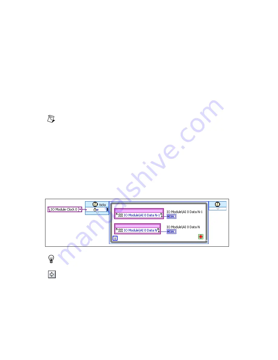
18. Drag 

AI 0 Data N and AI 0 Data N-1 

to the block diagram.

19. Add a Timed Loop structure around the two nodes.

20. Wire indicators to the output terminals of the

 IO Module\AI 0 Data N

 and 

IO Module\AI 0 Data 

N-1 

nodes.

21. Wire an 

FPGA Clock Constant

 to the input node of the Timed Loop. Set this constant to 

IO Module Clock 0

.

Your block diagram should now resemble the block diagram in Figure 6.

Figure 6.  

5762SampleAcq (FPGA).vi Block Diagram

Tip

Click the 

Clean Up Diagram

 button on the toolbar to cleanly organize the VI block diagrams.

22. Save the VI as 

5762SampleAcq (FPGA).vi

.

23. Click the 

Run

 button. LabVIEW creates a default build specification and begins compiling the VI. 

The 

Generating Intermediate Files

 window opens and displays the code generation progress. 

Next, the 

Compilation Status 

window opens and displays the progress of the compilation. The 

compilation takes several minutes.

24. Click 

Close 

in the 

Compilation Status 

window.

Summary of Contents for 5762R

Page 1: ...bVIEW project with the NI 5762R Contents Electromagnetic Compatibility Guidelines 2 How to Use Your NI FlexRIO Documentation Set 3 Front Panel and Connector Pinouts 4 Block Diagram 6 NI 5762 Component...

Page 2: ...nges or modifications to the product not expressly approved by National Instruments could void your authority to operate it under your local regulatory rules Caution To ensure the specified EMC perfor...

Page 3: ...LabVIEW FPGA Module Help Embedded in LabVIEW Help Contains information about the basic functionality of LabVIEW FPGA Module NI FlexRIO Help Embedded in LabVIEW FPGA Module Help Contains FPGA module a...

Page 4: ...evice and the chassis NI is not liable for any damage resulting from such signal connections For the maximum input and output ratings for each signal refer to the Specifications section of this docume...

Page 5: ...ata channel 4 DIO Port 0 2 Bidirectional single ended digital I O data channel 5 GND Ground reference for signals 6 DIO Port 0 3 Bidirectional single ended digital I O data channel 7 DIO Port 1 0 Bidi...

Page 6: ...Trigger Input Sync Clock IoModSyncClk PLL Locked Initialization Done Reinitialize AI 0 Data Over Range AI 1 Data Over Range 16 16 Configuration Error Configuration Error Code SPI Device Select SPI Re...

Page 7: ...integration functionality of the user defined CLIP but it also allows the CLIP to communicate directly with circuitry external to the FPGA Adapter module socketed CLIP allows your IP to communicate d...

Page 8: ...ports of four signals each and are accessed using a U8 data type and Boolean write enable signal The four PFI signals are accessed individually using Boolean controls The NI 5762 Multiple Sample CLIP...

Page 9: ...VIEW FPGA application This section explains how to use an existing LabVIEW FPGA example project to generate and acquire samples with the NI 5762R This example requires at least one SMA cable for conne...

Page 10: ...right click the Open FPGA VI Reference PXI 7952R function and select Configure Open FPGA VI Reference c In the Configure Open FPGA VI Reference dialog box click the Browse button next to the Bitfile b...

Page 11: ...ct and click OK The new project opens in the Project Explorer window 3 Save the project as 5762SampleAcq lvproj Creating an FPGA Target VI 1 In the Project Explorer window right click My Computer and...

Page 12: ...information about configuring your clocks 15 In the Project Explorer window right click the FPGA target and select New VI A blank VI opens 16 Select Window Show Block Diagram to open the VI block dia...

Page 13: ...nd select Create Control to create a STOP button on the VI front panel window 10 Add the Read Write Control function located on the FPGA Interface palette inside the While Loop 11 Wire the FPGA VI Ref...

Page 14: ...ure 7 Figure 7 5762SampleAcq Host vi Block Diagram 19 Save the VI as 5762SampleAcq Host vi Running the Host VI 1 Connect one end of an SMA cable to AI 0 on the front panel of the NI 5762 and the other...

Page 15: ...an NI 5762 Typical values describe useful product performance that are not covered by warranty Typical values cover the expected performance of units over ambient temperature ranges of 23 5 C with an...

Page 16: ...imum voltage 3 V DC 5 Vpk pk AC Measurements Figure 8 Frequency Response Logarithmic Scale Table 5 Bandwidth 3 dB Device Lower 3 dB Frequency Upper 3 dB Frequency NI 5762 01 61 7 kHz 102 MHz NI 5762 0...

Page 17: ...ency Response NI 5762 01 only Logarithmic Scale Figure 10 Frequency Response NI 5762 02 only Logarithmic Scale 80 90 100110120 Frequency MHz dBFS 0 1 2 3 4 5 1 5 10 20 30 40 50 60 70 NI 5762 01 6 0 2...

Page 18: ...Figure 12 Single Tone Spectrum at 20 MHz 3 1 dBFS SFDR 90 8 dBc NI 5762 01 and NI 5762 02 0 10 20 30 40 50 60 70 80 90 0 50 150 Frequency MHz dBFS 200 250 100 NI 5762 01 NI 5762 02 0 110 130 0 10 40 F...

Page 19: ...NR at 10 1 MHz 1 dBFS 74 6 dBc 1 dBFS 75 8 dBc SINAD at 10 1 MHz 1 dBFS 73 3 dBc 1 dBFS 75 2 dBc SFDR at 10 1 MHz with harmonics 6 dBFS 88 2 dBc 3 dBFS 88 4 dBc SFDR at 10 1 MHz without harmonics 6 dB...

Page 20: ...ernal stability 1 ppm CLK IN Number of channels 1 single ended Connector type SMA Input impedance 50 Input coupling AC Input voltage range 0 63 Vpk pk to 2 0 Vpk pk Absolute maximum voltage 3 0 V DC 3...

Page 21: ...out the supported analog input ranges and buffer currents refer to pages 19 and 23 of the AD9467 data sheet available at www analog com TRIG General Characteristics Number of channels 1 single ended C...

Page 22: ...ce with IEC 60068 2 1 and IEC 60068 2 2 Relative humidity range 10 to 90 noncondensing tested in accordance with IEC 60068 2 56 Altitude 2 000 m at 25 C ambient temperature Pollution Degree 2 Storage...

Page 23: ...er safety certifications refer to the product label or the Online Product Certification section Electromagnetic Compatibility This product meets the requirements of the following EMC standards for ele...

Page 24: ...ment visit ni com environment weee Where to Go for Support The National Instruments Web site is your complete resource for technical support At ni com support you have access to everything from troubl...

Page 25: ...e following instructions to install PXI EMC filler panels National Instruments part number 778700 01 in your PXI chassis 1 Remove the captive screw covers 2 Install the PXI EMC filler panels by securi...

Page 26: ...on your media or the National Instruments Patent Notice at ni com patents Refer to the Export Compliance Information at ni com legal export compliance for the National Instruments global trade compli...

Reviews: