

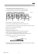


Temperature
Compensating Type
High Dielectric
Constant Type
10
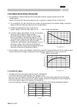
Adhesive Strength
No removal of the terminations or other defect should occur.
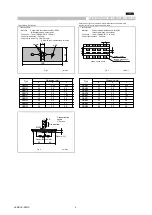
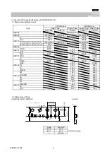
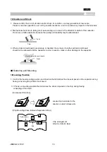
Solder the capacitor on the test jig (glass epoxy board)shown in
of Termination
Fig.3 using an eutectic solder. Then apply 10N* force in parallel
with the test jig for 10±1seconds.
The soldering should be done either with an iron or using the
reflow method and should be conducted with care so that the
soldering is uniform and free of defects such as heat shock.
*1N(GRM02),2N(GRM03),5N(GRM15,GRM18)
11
Vibration
Appearance No defects or abnormalities.
Solder the capacitor on the test jig (glass epoxy board) in the same
Resistance
manner and under the same conditions as (10).
Capacitance Within the specified tolerance.
The capacitor should be subjected to a simple harmonic motion
having a total amplitude of 1.5mm, the frequency being varied
Q/D.F.
30pF and over:Q
≧
1000
[B1,B3,R1,R6,R7,C7,C8,L8]
uniformly between the approximate limits of 10 and 55Hz. The
30pF and beloow:Q
≧
400+20C
W.V.:100V :0.025max.(C
<
0.068
m
F)
frequency range, from 10 to 55Hz and return to 10Hz, should be
:0.05max.(C
≧
0.068
m
F)
traversed in approximately 1 minute. This motion should be
C:Nominal Capacitance(pF)
W.V.:50V/25V :0.025max.
applied for a period of 2 hours in each 3 mutually perpendicular
W.V.:16V/10V :0.035max.
directions(total of 6 hours).
W.V.:6.3V/4V :0.05max. (C
<
3.3
m
F)
:0.1max.(C
≧
3.3
m
F)
[R9]
W.V.:50V: 0.05max.
[F1,F5]
W.V.:25Vmin
:0.05max. (C
<
0.1
m
F)
:0.09max. (C
≧
0.1
m
F)
W.V.:16V/10V:0.125max.
W.V.:6.3V:0.15max.
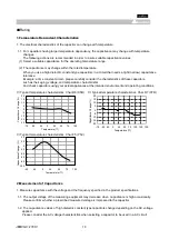
12
Deflection
Appearance No defects or abnormalities.
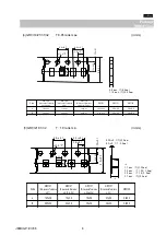
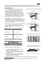
Solder the capacitor on the test jig (glass epoxy board) shown in
Fig.1 using an eutectic solder. Then apply a force in the direction
Capacitance Within ±5% or± 0.5pF
Within ±10%
shown in Fig 2 for 5±1 seconds. The soldering should be done
Change
(Whichever is larger)
by the reflow method and should be conducted with care so that
the soldering is uniform and free of defects such as heat shock.
13
Solderability
75% of the terminations is to be soldered evenly and continuously.
Immerse the capacitor in a solution of ethanol (JIS-K-8101) and
of Termination
rosin (JIS-K-5902) (25% rosin in weight propotion) .
Preheat at 80 to 120
℃
for 10-to 30 seconds.
After preheating, immerse in an eutectic solder solution for
2±0.5 seconds at 230±5
℃
or Sn-3.0Ag-0.5Cu solder solution
for 2
±
0.5 seconds at 245±5
℃
.
14
Resistance to
Appearance No defects or abnormalities.
Preheat the capacitor at 120 to 150
℃
for 1 minute.
Soldering Heat
Immerse the capacitor in an eutectic solder solution* or
Capacitance Within
±
2.5% or
±
0.25pF
B1,B3,R1,R6,R7,R9,C7,C8,L8:Within
±
7.5%
Sn-3.0Ag-0.5Cu solder solution at 270±5
℃
for 10±0.5 seconds.
Change
(Whichever is larger)
F1,F5 :Within
±
20%
Set at room temperature for 24±2 hours, then measure.
Q/D.F.
30pF and over:Q
≧
1000
[
B1,B3,R1,R6,R7,C7,C8,L8
]
*Not apply to GRM02
30pF and beloow:Q
≧
400+20C W.V.:100V :0.025max.(C
<
0.068
m
F)
:0.05max.(C
≧
0.068
m
F)
· Initial measurement for high dielectric constant type
C:Nominal Capacitance(pF)
W.V.:50V/25V :0.025max.
Perform a heat treatment at 150+0/-10
C for one hour and then set
W.V.:16V/10V :0.035max.
at room temperature for 24±2 hours.
W.V.:6.3V/4V :0.05max. (C
<
3.3
m
F)
Perform the initial measurement.
:0.1max.(C
≧
3.3
m
F)
[R9]
*Preheating for GRM32/43/55
W.V.:50V: 0.05max.
[F1,F5]
W.V.:25Vmin
:0.05max. (C
<
0.1
m
F)
:0.09max. (C
≧
0.1
m
F)
W.V.:16V/10V:0.125max.
W.V.:6.3V:0.15max.
I.R.
More than 10,000M
W
or 500
W
·F(Whichever is smaller)
Dielectric
No defects.
Strength
15
Temperature
Appearance No defects or abnormalities.
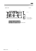
Fix the capacitor to the supporting jig in the same
Cycle
manner and under the same conditions as (10).
Capacitance Within
±
2.5% or
±
0.25pF
B1,B3,R1,R6,R7,R9,C7,C8,L8:Within
±
7.5%
Perform the five cycles according to the four heat
Change
(Whichever is larger)
F1,F5 :Within
±
20%
treatments shown in the following table.
Q/D.F.
30pF and over:Q
≧
1000
[
B1,B3,R1,R6,R7,C7,C8,L8
]
Set for 24±2 hours at room temperature, then measure.
30pF and beloow:Q
≧
400+20C W.V.:100V :0.025max.(C
<
0.068
m
F)
:0.05max.(C
≧
0.068
m
F)
C:Nominal Capacitance(pF)
W.V.:50V/25V :0.025max.
W.V.:16V/10V :0.035max.
W.V.:6.3V/4V :0.05max. (C
<
3.3
m
F)
:0.1max.(C
≧
3.3
m
F)
[R9]
W.V.:50V: 0.05max.
[F1,F5]
W.V.:25Vmin
· Initial measurement for high dielectric constant type
:0.05max. (C
<
0.1
m
F)
Perform a heat treatment at 150+0/-10
C for one hour and then set
:0.09max. (C
≧
0.1
m
F)
at room temperature for 24±2 hours.
W.V.:16V/10V:0.125max.
Perform the initial measurement.
W.V.:6.3V:0.15max.
I.R.
More than 10,000M
W
or 500
W
·F(Whichever is smaller)
Dielectric
No defects.
Strength
■
SPECIFICATIONS AND TEST METHODS
No
Item
Specification
Test Method
Table1
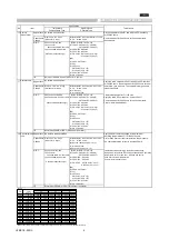
Step
Temperature
Time
1
100
C to 120
C
1 min.
2
170
C to 200
C
1 min.
Step
Temp.(
C)
Time (min)
1
Min.
Operating Temp.+0/-3
30±3
2
Room Temp
2 to 3
3
Max.
Operating Temp.+3/-0
30±3
4
Room Temp
2 to 3
JEMCGS-0001S
3


