HARDWARE AND SPECIFICATIONS
10
Dragonfly
™
Nano MTQN-MNG3-B01 Device Guide
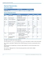
Electrical Characteristics
Operating Conditions
Parameter
Minimum Volts
Maximum Volts
Supply Range - Vcc
3.2
5.25
Absolute Maximum Ratings
Symbol
Description
Conditions
Min.
Max.
Unit
SIM
SIM interface
Input DC voltage at SIM digital
interfaces pins
-0.3
3.9
V
P_ANT
Antenna power
Input RF power at ANT pin
-22
dbM
Rho_ANT
Antenna ruggedness
Output RF load mismatch
ruggedness at ANT pins
10.1
VSWR
tstg
Storage Temperature
-40
85
°C
V
P
Voltage at any pin
Voltage at any signal pin
-0.3
4
V
V
DDX
- V
SS
External voltage
V
DDX
, V
DDA
,V
DDIO2
, V
BAT
1
-0.3
4
V
V
IN
2
Input Voltage
Input voltage on FT_xxx pins
V
SS
-0.3
min (V
DD
,
V
DDA
,V
DDIO2
)+
4.0
3 & 4
V
Input voltage on TT_xx pins
V
SS
-0.3
4.0
V
Input voltage on BOOT0 pin
V
SS
9.0
V
Input voltage on any other pins V
SS
-0.3
4.0
V
|
Δ
V
DDx|
Variations between
power pins
Variations between
different V
DDX
power pins of
the same domain
N/A
50
mV
|V
SSx
-V
SS
|
Variations between
ground pins
Variations between all the
different ground pins
5
N/A
50
mV
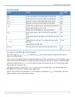
Data taken from STM32L471QG processor datasheet.
(1) All main power (V
DD
, V
DDA
, V
DDIO2
, V
BAT
) and ground (V
SS
, V
SSA
) pins must always be connected to the external power
(2) V
IN
maximum must always be respected. Refer to Nominal Ratings for the maximum allowed injected current
values.
(3) This formula has to be applied only on the power supplies related to the IO structure described in the pin
definition table.
(4) To sustain a voltage higher than 4 V the internal pull-up/pull-down resistors must be disabled.
(5) Include VREF- pin.

