Motorola NXP SYMPHONY DSP56007 Technical Data Manual Download Page 1


MOTOROLA


SEMICONDUCTOR TECHNICAL DATA


DSP56007


Order this document by:

DSP56007/D

©1996, 1997 MOTOROLA, INC.


SYMPHONY


 AUDIO DSP FAMILY

24-BIT DIGITAL SIGNAL PROCESSORS


Motorola designed the Symphony


 family of high-performance, programmable Digital Signal 

Processors (DSPs) to support a variety of digital audio applications, including Dolby ProLogic, 
ATRAC, and Lucasfilm Home THX processing. Software for these applications is licensed by 
Motorola for integration into products like audio/video receivers, televisions, and automotive 
sound systems with such user-developed features as digital equalization and sound field 
processing. The DSP56007 is an MPU-style general purpose DSP, composed of an efficient 24-bit 
Digital Signal Processor core, program and data memories, various peripherals optimized for 
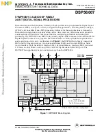
audio, and support circuitry. As illustrated in 


Figure 1


, the DSP56000 core family compatible 

DSP is fed by program memory, two independent data RAMs and two data ROMs, a Serial 
Audio Interface (SAI), Serial Host Interface (SHI), External Memory Interface (EMI), dedicated 
I/O lines, on-chip Phase Lock Loop (PLL), and On-Chip Emulation (OnCE


) port. The 

DSP56007 has significantly more on-chip memory than the DSP56004.


ˇ


Figure 1  


DSP56007 Block Diagram

Y Data 

Memory*

X Data 

Memory*

Program 

Memory*

Program Control Unit

24-Bit

DSP56000 

Core

OnCE

TM

 Port

PLL

Clock

Gen.

4

9

5

29

16-Bit Bus
24-Bit Bus

Data ALU

24 

×

 24 + 56 

 56-Bit MAC

Two 56-Bit Accumulators

Interrupt

 Control

Program 

Decode 

Controller

Program 

Address 

Generator

4

IRQA, IRQB, NMI, RESET

4

3

Internal 

Data

 Bus 

Switch

Address

Generation 

Unit

Refer to Table 1 for memory configurations.

*

PAB

XAB

YAB

GDB

PDB

XDB

YDB

General 

Purpose 

Input/ 

Output

External 
Memory 

Interface

 (EMI)

Serial 
Audio 

Interface 

(SAI)

Serial 

Host 

Interface 

(SHI)

AA0248


F

re

e

sc

a

le

 S

e

m

ic

o

n

d

u

c

to

r,

 I


Freescale Semiconductor, Inc.

For More Information On This Product,

   Go to: www.freescale.com

n

c

.

..

Summary of Contents for NXP SYMPHONY DSP56007

Page 1: ...in Figure 1 the DSP56000 core family compatible DSP is fed by program memory two independent data RAMs and two data ROMs a Serial Audio Interface SAI Serial Host Interface SHI External Memory Interface EMI dedicated I O lines on chip Phase Lock Loop PLL and On Chip Emulation OnCE port The DSP56007 has significantly more on chip memory than the DSP56004 ˇ Figure 1 DSP56007 Block Diagram Y Data Memo...

Page 2: ...ive when pulled low For example the RESET pin is active when low asserted Means that a high true active high signal is high or that a low true active low signal is low deasserted Means that a high true active high signal is low or that a low true active low signal is high Examples Signal Symbol Logic State Signal State Voltage PIN True Asserted VIL VOL PIN False Deasserted VIH VOH PIN True Asserte...

Page 3: ...ecision arithmetic Hardware support for block floating point Fast Fourier Transforms FFT Hardware nested DO loops Zero overhead fast interrupts 2 instruction cycles Four 24 bit internal data buses and three 16 bit internal address buses for simultaneous accesses to one program and two data memories Fabricated in high density CMOS Memory On chip modified Harvard architecture which permits simultane...

Page 4: ...16 20 or 24 bits wide Four dedicated independent programmable General Purpose Input Output GPIO lines On chip peripheral registers memory mapped in data memory space Three external interrupt request pins On Chip Emulation OnCE port for unobtrusive processor speed independent debugging Software programmable Phase Lock Loop based PLL frequency synthesizer for the core clock Power saving Wait and Sto...

Page 5: ...ola DSP home page on the Internet the source for the latest information Table 2 DSP56007 Documentation Document Name Description of Content Order Number DSP56000 Family Manual DSP56000 core family architecture and the 24 bit core processor and instruction set DSP56KFAMUM AD DSP56007 User s Manual Memory peripherals and interfaces DSP56007UM AD DSP56007 Technical Data Electrical and timing specific...

Page 6: ...vi DSP56007 D MOTOROLA DSP56007 Product Documentation Freescale Semiconductor I Freescale Semiconductor Inc For More Information On This Product Go to www freescale com nc ...

Page 7: ...mber of Signals Detailed Description Power VCC 9 Table 1 2 Ground GND 13 Table 1 3 Phase Lock Loop PLL 3 Table 1 4 External Memory Interface EMI 29 Table 1 5 and Table 1 6 Interrupt and Mode Control 4 Table 1 7 Serial Host Interface SHI 5 Table 1 8 Serial Audio Interface SAI 9 Table 1 9 and Table 1 10 General Purpose Input Output GPIO 4 Table 1 11 On Chip Emulation OnCE port 4 Table 1 12 Total 80 ...

Page 8: ...E Port C Port B Port A External Memory Mode Interrupt 80 signals Serial Host Rec0 SDO1 Tran1 WST SCKT SDO0 Tran0 Interface MRD MCS0 Serial Audio Interface Interface MOSI HA0 SDO2 Tran2 SDI1 Rec1 GPIO0 GPIO3 GPIO HREQ VCCP GNDP PCAP PLL PINIT MA15 MCS3 EXTAL GNDA VCCA GNDD VCCD Reset AA0249G Port Power Inputs Ground Control 2 2 3 3 4 2 3 8 4 15 DSP56007 Freescale Semiconductor I Freescale Semicondu...

Page 9: ...quate external decoupling capacitors Table 1 3 Grounds Ground Name Description GNDP PLL Ground GNDP is ground dedicated for PLL use The connection should be provided with an extremely low impedance path to ground VCCP should be bypassed to GNDP by a 0 47 µF capacitor located as close as possible to the chip package GNDQ Quiet Ground GNDQ provides isolated ground for the internal processing logic T...

Page 10: ...the four phase instruction cycle clock PCAP Input Input PLL Filter Capacitor This input is used to connect a high quality high Q factor external capacitor needed for the PLL filter The capacitor should be as close as possible to the DSP with heavy short traces connecting one terminal of the capacitor to PCAP and the other terminal to VCCP The required capacitor value is specified in Table 2 6 on p...

Page 11: ... as memory chip select 2 for SRAM accesses Memory Chip Select 2 MCS2 For SRAM access this line functions as memory chip select 2 Memory Column Address Strobe MCAS This line functions as the Memory Column Address Strobe MCAS during DRAM accesses MA17 MCS1 MRAS Output Table 1 6 Memory Address Line 17 MA17 This line functions as the non multiplexed address line 17 Memory Chip Select 1 MCS1 This line ...

Page 12: ... Driven High Driven High Previous State Driven High Previous State Driven High MA16 MCS2 MCAS DRAM refresh disabled DRAM refresh enabled Driven High Driven High Driven High Driven High Driven High Driven High Driven High Driven High Previous State Driven High Driven High Driven Low Previous State Driven High Driven High Driven High MA17 MCS1 MRAS DRAM refresh disabled DRAM refresh enabled Driven H...

Page 13: ...e The logic state present on the MODA MODB and MODC pins selects the initial DSP operating mode Several clock cycles after leaving the Reset state the MODA signal changes to the external interrupt request IRQA The DSP operating mode can be changed by software after reset External Interrupt Request A IRQA The IRQA input is a synchronized external interrupt request It may be programmed to be level s...

Page 14: ...pt request IRQB The DSP operating mode can be changed by software after reset External Interrupt Request B IRQB The IRQB input is a synchronized external interrupt request It may be programmed to be level sensitive or negative edge triggered When the signal is edge triggered triggering occurs at a voltage level and is not directly related to the fall time of the interrupt signal However as the fal...

Page 15: ...the probability that noise on NMI will generate multiple interrupts also increases Hardware reset causes this input to function as MODC RESET input active RESET This input causes a direct hardware reset of the processor When RESET is asserted the DSP is initialized and placed in the Reset state A Schmitt trigger input is used for noise immunity When the reset signal is deasserted the initial DSP o...

Page 16: ... SPI if it is defined as a slave and the Slave Select SS signal is not asserted In both the master and slave SPI devices data is shifted on one edge of the SCK signal and is sampled on the opposite edge where data is stable Edge polarity is determined by the SPI transfer protocol I2 C Serial Clock SCL SCL carries the clock for bus transactions in the I2 C mode SCL is a Schmitt trigger input when c...

Page 17: ...que situation and is defined as the Start event A low to high transition of SDA while SCL is high is an unique situation and is defined as the Stop event Note This line is tri stated during hardware reset software reset or individual reset no need for external pull up in this state MOSI HA0 Input or Output Input Tri stated SPI Master Out Slave In MOSI When the SPI is configured as a master MOSI is...

Page 18: ...o need for external pull up in this state HREQ Input or Output Tri stated Host Request This signal is an active low Schmitt trigger input when configured for the Master mode but an active low output when configured for the Slave mode When configured for the Slave mode HREQ is asserted to indicate that the SHI is ready for the next data word transfer and deasserted at the first clock pulse of the n...

Page 19: ...l Data Input 1 While in the high impedance state the internal input buffer is disconnected from the pin and no external pull up is necessary SDI1 is the serial data input for receiver 1 Note This signal is high impedance during hardware or software reset while receiver 1 is disabled R1EN 0 or while the DSP is in the Stop state SCKR Input or Output Tri stated Receive Serial Clock SCKR is an output ...

Page 20: ...e data sample Note WSR is high impedance if all receivers are disabled individual reset during hardware reset during software reset or while the DSP is in the Stop state While in the high impedance state the internal input buffer is disconnected from the signal and no external pull up is necessary Table 1 9 Serial Audio Interface SAI Receiver signals Continued Signal Name Signal Type State during ...

Page 21: ...ut if the transmit section is configured as a master or a Schmitt trigger input if the transmit section is configured as a slave When the SCKT is an output it provides an internally generated SAI transmit clock to external circuitry When the SCKT is an input it allows external circuitry to clock data out of the SAI Note SCKT is high impedance if all transmitters are disabled individual reset durin...

Page 22: ...gnals Signal Name Signal Type Stateduring Reset Signal Description DSI OS0 Input Output Output Driven Low Debug Serial Input DSI The DSI signal is the signal through which serial data or commands are provided to the OnCE port controller The data received on the DSI signal will be recognized only when the DSP has entered the Debug mode of operation Data must have valid TTL logic levels before the s...

Page 23: ...e DSO line provides the data contained in one of the OnCE port controller registers as specified by the last command received from the command controller The Most Significant Bit MSB of the data word is always shifted out of the OnCE port first Data is clocked out of the OnCE port on the rising edge of DSCK The DSO line also provides acknowledge pulses to the external command controller When the D...

Page 24: ...sary to reset the OnCE port controller in cases where synchronization between the OnCE port controller and external circuitry is lost Asserting DR when the DSP is in the Wait or the Stop mode and keeping it asserted until an acknowledge pulse in the DSP is produced puts the DSP into the Debug mode After receiving the acknowledge pulse DR must be deasserted before sending the first OnCE port comman...

Page 25: ...ated using the worst case for the same parameters in the opposite direction Therefore a maximum value for a specification will never occur in the same device that has a minimum value for another specification adding a maximum to a minimum represents a condition that can never exist CAUTION This device contains circuitry protecting against damage due to high static voltage or electrical fields howe...

Page 26: ...2 7 C W Notes 1 Junction to ambient thermal resistance is based on measurements on a horizontal single sided Printed Circuit Board per SEMI G38 87 in natural convection SEMI is Semiconductor Equipment and Materials International 805 East Middlefield Rd Mountain View CA 94043 415 964 5111 2 Junction to case thermal resistance is based on measurements using a cold plate per SEMI G30 88 with the exce...

Page 27: ... inputs1 All other inputs VILC VILM VILS VIL 0 5 0 5 0 5 0 5 0 4 2 0 0 3 VCC 0 8 0 5 0 5 0 5 0 5 0 4 2 0 0 3 VCC 0 8 0 5 0 5 0 5 0 5 0 4 2 0 0 3 VCC 0 8 V V V V Input leakage current EXTAL RESET MODA MODB MODC DR Other Input Pins 2 4 V 0 4 V IIN 1 10 1 10 1 10 1 10 1 10 1 10 µA µA High impedance off state input current 2 4 V 0 4 V ITSI 10 10 10 10 10 10 µA Output high voltage IOH 0 4 mA VOH 2 4 2 ...

Page 28: ... 50 pF the drive capability of the output pins typically decreases linearly 1 At 1 5 ns per 10 pF of additional capacitance at all output pins except MOSI HA0 MISO SDA SCK SCL HREQ 2 At 1 0 ns per 10 pF of additional capacitance at output pins MOSI HA0 MISO SDA SCK SCL HREQ in SPI mode only PLL supply current 0 7 1 1 1 0 1 5 1 3 2 2 mA Input capacitance3 CIN 10 10 10 pF Notes 1 The SHI inputs are ...

Page 29: ...n 0 48 TC Max 0 52 TC Min 0 467 TC Max 0 533 TC Internal Clock Low Period with PLL disabled with PLL enabled and MF 4 with PLL enabled and MF 4 TL ETL Min 0 48 TC Max 0 52 TC Min 0 467 TC Max 0 533 TC Internal Clock Cycle Time TC DF MF ETC Instruction Cycle Time ICYC 2 TC Table 2 5 External Clock EXTAL Pin No Characteristics Sym 50 MHz 66 MHz 88 MHz Unit Min Max Min Max Min Max Frequency of Extern...

Page 30: ...50 of the input transition Figure 2 1 External Clock Timing Table 2 6 Phase Lock Loop PLL Characteristics Characteristics Expression Min Max Unit VCO frequency when PLL enabled MF Ef 10 f1 MHz PLL external capacitor PCAP pin to VCCP MF CPCAP 1 MF 4 MF 4 MF 340 MF 380 MF 480 MF 970 pF pF Note 1 Cpcap is the value of the PLL capacitor connected between PCAP pin and VCCP for MF 1 The recommended valu...

Page 31: ...it 17 1 6 TC TL 12 ns ns Note 1 This timing requirement is sensitive to the quality of the external PLL capacitor connected to the PCAP pin For capacitor values less than or equal to 2 nF asserting RESET according to this timing requirement will ensure proper processor initialization for capacitors with a deltaC C less than 0 5 This is typical for ceramic capacitors For capacitor values greater th...

Page 32: ...igure 2 6 Recovery from Stop State Using IRQA Figure 2 7 Recovery from Stop State Using IRQA Interrupt Service VIHM VILM VIH VIL RESET MODA MODB MODC VIHR IRQA IRQB NMI 14 15 AA0252 IRQA IRQB NMI 16 16A IRQA IRQB NMI AA0253 General Purpose I O General Purpose I O Output IRQA IRQB NMI 22 18 AA0254 IRQA 25 AA0255 IRQA AA0256 27 Freescale Semiconductor I Freescale Semiconductor Inc For More Informati...

Page 33: ... Mode Access Only tRASP slow fast 3 TC 11 n 4 TC 2 TC 11 n 3 TC 209 149 156 110 114 79 9 ns ns 47 RAS Assertion Pulse Width Single Access Only tRAS slow fast 7 TC 11 5 TC 11 129 89 95 65 68 5 45 8 ns ns 48 RAS or CAS Deassertation to RAS Assertion tRP TCRP slow fast 5 TC 5 3 TC 5 95 55 70 40 51 8 29 1 ns ns 49 CAS Assertion Pulse Width TCAS slow fast 3 TC 10 2 TC 10 50 30 35 20 24 1 12 7 ns ns 50 ...

Page 34: ...to Column Address Not Valid Column Address Hold Time TCAH slow fast 7 TC TH 14 4 TC TH 14 136 76 100 54 71 2 37 1 ns ns 60 RAS Assertion to Column Address Not Valid tAR slow fast 7 TC TH 14 5 TC TH 14 136 96 100 69 71 2 48 5 ns ns 61 Column Address Valid to RAS Deassertation tRAL slow fast 3 TC TL 7 2 TC TL 7 63 43 46 30 32 8 21 2 ns ns 62 CAS RAS RD or WR Deassertation to WR or RD Assertion tRCH ...

Page 35: ...s ns 70 WR Assertion to CAS Assertion tWCS slow fast 4 TC 14 3 TC 14 66 46 47 31 31 4 20 1 ns ns 71 WR Assertion Pulse Width Single Cycle Only tWP slow fast 7 TC 9 5 TC 9 131 91 97 67 70 5 47 8 ns ns 72 RAS Assertion to WR Deassertation Single Cycle Only tWCR slow fast 7 TC 15 5 TC 15 125 85 91 61 64 5 41 8 ns ns 73 WR Assertion to Data Active slow fast 3 TC TH 13 2 TC TH 13 57 37 40 25 26 8 15 4 ...

Page 36: ... 8 DRAM Single Read Cycle MRAS MCAS MA0 MA10 MWR MRD MD0 MD7 Data In Row Address Last Column Address 47 48 64 48 74 52 65 50 49 55 53 59 60 56 62 57 61 43 42 63 45 AA0257 44 Freescale Semiconductor I Freescale Semiconductor Inc For More Information On This Product Go to www freescale com nc ...

Page 37: ...Address Col Address Last Column Address 48 46 60 50 48 65 41 54 52 54 49 49 49 61 59 58 58 53 51 55 56 57 57 57 62 43 44 44 44 43 43 Data 42 63 63 63 45 45 45 In Data In Data In MRAS MCAS MA0 MA10 MWR MRD MD0 MD7 AA0263 Freescale Semiconductor I Freescale Semiconductor Inc For More Information On This Product Go to www freescale com nc ...

Page 38: ... DRAM Single Write Cycle 47 48 48 Row Address Column Address 64 Data Out 74 52 50 49 55 53 61 59 60 65 56 57 62 66 70 72 71 69 68 67 73 MRAS MCAS MA0 MA10 MWR MRD MD0 MD7 AA0264 Freescale Semiconductor I Freescale Semiconductor Inc For More Information On This Product Go to www freescale com nc ...

Page 39: ...Row Address Col Address Last Column Address 48 46 60 50 48 65 41 54 52 54 49 49 49 61 59 58 58 53 51 55 56 57 57 57 62 Data Out 69 68 68 67 73 67 Data Out Data Out MRAS MCAS MA0 MA10 MWR MRD MD0 MD7 AA0265 70 66 68 67 Freescale Semiconductor I Freescale Semiconductor Inc For More Information On This Product Go to www freescale com nc ...

Page 40: ...n Pulse Width tRAS slow fast1 7 TC 9 5 TC 9 131 91 97 70 5 ns ns 85 RAS Deassertation to RAS Assertion for Refresh Cycle2 tRP slow fast1 5 TC 5 3 TC 5 95 55 70 51 8 ns ns 86 CAS Assertion to RAS Assertion on Refresh Cycle TCSR TC 7 13 8 4 4 ns 87 RAS Assertion to CAS Deassertation on Refresh Cycle TCHR slow fast1 7 TC 15 5 TC 15 125 85 91 64 5 ns ns 88 RAS Deassertation to CAS Assertion on a Refre...

Page 41: ...r WR Assertion tAS TC TL 13 17 10 4 4 ns 93 RD or WR Assertion Pulse Width tWP 2 TC 5 Ws TC 35 23 17 7 ns 94 RD or WR Deassertation to RD or WR Assertion 2 TC 11 29 19 11 7 ns 95 RD or WR Deassertation to Address not Valid tWR TH 6 4 2 0 1 ns 96 Address Valid to Input Data Valid tAA tAC 3 TC TL 15 Ws TC 55 38 24 8 ns 97 RD Assertion to Input Data Valid tOE 2 TC 15 Ws TC 25 15 7 7 ns 98 RD Deassert...

Page 42: ...ertation to Data high impedance1 TH 10 20 18 15 7 ns 104 WR Assertion to Data Active TH 6 4 2 0 1 ns Note 1 This value is periodically sampled and not 100 tested Figure 2 13 SRAM Read Cycle Table 2 10 External Memory Interface EMI SRAM Timing No Characteristics Symbol Expression 50 MHz 66 MHz 88 MHz Unit Min Max Min Max Min Max MA0 MA14 MA15 MCS3 MA16 MCS2 MCAS MA17 MCS1 MRAS MCS0 RD WR Data In MD...

Page 43: ... 2 19 Figure 2 14 SRAM Write Cycle MA0 MA14 MA15 MCS3 MA16 MCS2 MCAS MA17 MCS1 MRAS MCS0 WR RD Data Out MD0 MD7 91 92 94 93 95 94 103 100 AA0268 99 102 104 101 Freescale Semiconductor I Freescale Semiconductor Inc For More Information On This Product Go to www freescale com nc ...

Page 44: ...Not Valid Data In Hold Time master slave 0 14 0 14 0 14 0 14 ns ns 117 SCKR Edge to Word Select Out Valid WSR Out Delay Time master 20 20 20 20 ns 118 Word Select In Valid to SCKR Edge WSR In Set up Time slave 12 12 12 12 ns 119 SCKR Edge to Word Select In Not Valid WSR In Hold Time slave 12 12 12 12 ns 121 SCKT Edge to Data Out Valid Data Out Delay Time master slave1 slave2 13 40 TH 34 13 40 44 1...

Page 45: ...15 SAI Receiver Timing SCKR RCKP 1 SCKR RCKP 0 Valid Valid WSR Output WSR Input SDI0 SDI1 Data Input 111 112 113 111 113 114 114 112 116 115 118 119 117 AA0269 114 114 Freescale Semiconductor I Freescale Semiconductor Inc For More Information On This Product Go to www freescale com nc ...

Page 46: ... 2 16 SAI Transmitter Timing Valid 111 112 113 111 113 114 114 112 121 123 124 122 AA0270 114 114 SCKT TCKP 1 SCKT TCKP 0 WST Output WST Input SDO0 SDO2 Data Output Freescale Semiconductor I Freescale Semiconductor Inc For More Information On This Product Go to www freescale com nc ...

Page 47: ...0 1000 2000 60 85 145 139 491 1082 91 1000 2000 45 70 130 124 476 1067 68 2 1000 2000 34 1 59 1 119 1 113 1 465 1 1056 1 ns ns ns ns ns ns ns ns ns ns 142 Serial Clock High Period CPHA 0 CPHA 12 CPHA 1 master slave slave bypassed narrow wide bypassed narrow wide 0 5 tSPICC 10 TC 8 TC 31 TC 43 TC TH 40 TC TH 216 TC TH 511 50 28 51 63 70 246 541 35 23 46 58 63 239 534 24 1 19 4 42 4 54 4 57 0 233 0 ...

Page 48: ...ta In Not Valid Data In Hold Time master slave bypassed narrow wide bypassed narrow wide 2 TC 17 2 TC 18 2 TC 28 2 TC 17 2 TC 18 2 TC 28 57 58 68 57 58 68 47 48 58 47 48 58 39 7 40 7 50 7 39 7 40 7 50 7 ns ns ns ns ns ns 150 SS Assertion to Data Out Active slave 4 4 4 4 ns 151 SS Deassertation to Data high impedance4 slave 24 24 24 24 ns 152 SCK Edge to Data Out Valid Data Out Delay Time CPHA 0 CP...

Page 49: ...CPHA 1 master 0 0 0 0 ns 163 First SCK Edge to HREQ In Not Asserted HREQ In Hold Time master 0 0 0 0 ns Note 1 For an Internal Clock frequency below 33 MHz the minimum permissible Internal Clock to Serial Clock frequency ratio is 4 1 For an Internal Clock frequency above 33 MHz the minimum permissible Internal Clock to Serial Clock frequency ratio is 6 1 2 In CPHA 1 mode the SPI slave supports dat...

Page 50: ...ing CPHA 0 SS Input SCK CPOL 0 Output SCK CPOL 1 Output MISO Input Valid MOSI Output MSB Valid LSB MSB LSB HREQ Input 141 142 143 144 144 141 144 144 143 142 148 149 149 148 152 153 163 161 AA0271 Freescale Semiconductor I Freescale Semiconductor Inc For More Information On This Product Go to www freescale com nc ...

Page 51: ...g CPHA 1 SS Input SCK CPOL 0 Output SCK CPOL 1 Output MISO Input Valid MOSI Output MSB Valid LSB MSB LSB HREQ Input 141 142 143 144 144 141 144 144 143 142 148 148 149 152 153 163 161 AA0272 162 149 Freescale Semiconductor I Freescale Semiconductor Inc For More Information On This Product Go to www freescale com nc ...

Page 52: ...Input SCK CPOL 0 Input SCK CPOL 1 Input MISO Output MOSI Input MSB LSB MSB LSB HREQ Output 141 142 143 144 144 141 144 144 143 142 154 150 152 153 148 149 159 157 AA0273 153 151 Valid Valid 148 149 147 160 146 Freescale Semiconductor I Freescale Semiconductor Inc For More Information On This Product Go to www freescale com nc ...

Page 53: ... 1 SS Input SCK CPOL 0 Input SCK CPOL 1 Input MISO Output MOSI Input MSB LSB MSB LSB HREQ Output 141 142 143 144 144 144 144 143 142 150 152 148 149 158 AA0274 153 151 Valid Valid 148 147 146 152 149 157 Freescale Semiconductor I Freescale Semiconductor Inc For More Information On This Product Go to www freescale com nc ...

Page 54: ...ock Cycle tSCL 10 0 µs 172 Bus Free Time tBUF 4 7 µs 173 Start Condition Set up Time tSU STA 4 7 µs 174 Start Condition Hold Time tHD STA 4 0 µs 175 SCL Low Period tLOW 4 7 µs 176 SCL High Period tHIGH 4 0 µs 177 SCL and SDA Rise Time tr 1 0 µs 178 SCL and SDA Fall Time tf 0 3 µs 179 Data Set up Time tSU DAT 250 ns 180 Data Hold Time tHD DAT 0 0 ns 182 SCL Low to Data Out Valid tVD DAT 3 4 µs 183 ...

Page 55: ...he actual maximum frequency is limited by the bus capacitances CL the pull up resistors RP which affect the rise and fall time of SDA and SCL see table below and by the input filters Consideration for programming the SHI Clock Control Register HCKR Clock Divide Ratio the master must generate a bus free time greater than T172 slave when operating with a DSP56007 SHI I2C slave The table below descri...

Page 56: ... 50 pF RP 2 kΩ No Char Sym Mode Filter Mode Expression 50 MHz2 66 MHz3 88 MHz4 U n i t Min Max Min Max Min Max Tolerable Spike Width on SCL or SDA bypassed narrow wide 0 20 100 0 20 100 0 20 100 0 20 100 ns ns ns 171 SCL Serial Clock Cycle tSCL master slave bypassed narrow wide bypassed narrow wide tI 2 CCP 3 TC 72 tr tI 2 CCP 3 TC 245 tr tI 2 CCP 3 TC 535 tr 4 TC TH 172 tr 4 TC TH 366 tr 4 TC TH ...

Page 57: ...igh Period tHIGH master slave bypassed narrow wide bypassed narrow wide 0 5 tI 2 CCP 2 TC 19 0 5 tI 2 CCP 2 TC 144 0 5 tI 2 CCP 2 TC 356 2 TC TH 1 2 TC TH 18 2 TC TH 30 379 544 776 49 68 80 375 523 773 37 56 68 360 507 754 27 4 46 4 58 4 ns ns ns ns ns ns 177 SCL Rise Time Output1 Input tr 1 7 RP CL 20 2000 238 2000 238 2000 238 2000 ns ns 178 SCL Fall Time Output1 Input tf 20 0 1 CL 50 2000 20 20...

Page 58: ... 0 0 0 ns ns ns 186 First SCL Sampling Edge to HREQ Output Deassertation slave bypassed narrow wide 3 TC TH 32 3 TC TH 209 3 TC TH 507 102 279 577 85 262 560 72 249 547 ns ns ns 187 Last SCL Edge to HREQ Output Not Deasserted slave bypassed narrow wide 2 TC TH 6 2 TC TH 63 2 TC TH 169 56 113 219 44 101 207 34 4 91 4 197 4 ns ns ns 188 HREQ In Assertion to First SCL Edge master bypassed narrow wide...

Page 59: ...d for the given bus load was used for the calculations in the Wide Filter mode 4 A tI 2 CCP of 56 TC the maximum permitted for the given bus load was used for the calculations in the Bypassed Filter mode A tI 2 CCP of 60 TC the maximum permitted for the given bus load was used for the calculations in the Narrow Filter mode A tI 2 CCP of 66 TC the maximum permitted for the given bus load was used f...

Page 60: ... to GPIO Out Not Valid GPIO Out Hold Time 2 2 ns 203 GPIO In Valid to EXTAL Edge GPIO In Set up Time 10 10 ns 204 EXTAL Edge to GPIO In Not Valid GPIO In Hold Time 6 6 ns Figure 2 22 GPIO Timing Valid GPIO 0 3 Input GPIO 0 3 Output EXTAL Input Note 1 Note 1 Valid when the ratio between EXTAL frequency and internal clock frequency equals 1 201 202 204 203 AA0276 Freescale Semiconductor I Freescale ...

Page 61: ... OS0 OS1 ACK Active 3 TC TL ns 239 DSO ACK Asserted to First DSCK High 2 TC ns 240 DSO ACK Assertion Width 4 TC TH 3 5 TC 7 ns 241 DSO ACK Asserted to OS0 OS1 High Impedance1 0 ns 242 OS0 OS1 Valid to EXTAL Transition 2 TC 21 ns 243 EXTAL Transition 2 to OS0 OS1 Invalid 0 ns 244 Last DSCK Low of Read Register to First DSCK High of Next Command 7 TC 10 ns 245 Last DSCK Low to DSO Invalid Hold 3 ns ...

Page 62: ...OP and enter Debug mode2 Stable External Clock OMR Bit 6 0 Stable External Clock OMR Bit 6 1 Stable External Clock PCTL Bit 17 1 65549 TC TL 21 TC TL 14 TC TL ns ns ns 251 DR Assertion to DSO ACK Valid Enter Debug mode After Recovery from STOP State2 Stable External Clock OMR Bit 6 0 Stable External Clock OMR Bit 6 1 Stable External Clock PCTL Bit 17 1 65553 TC TL 25 TC TL 18 TC TL ns ns ns Note 1...

Page 63: ...put DSO Output ACK OS1 DSI Input OS0 Note 1 Note 1 High Impedance external pull down resistor Last 236 237 238 AA0279 DSCK Input DSO Output OS0 Note 1 Note 1 High Impedance external pull down resistor Last 235 245 AA0280 234 Note 1 High Impedance external pull down resistor OS1 Output DSO Output DSCK Input OS0 Output Note 1 DSO Output DSI Input Note 1 241 239 240 241 236 237 AA0281 Freescale Semic...

Page 64: ...nchronous Recovery from WAIT State EXTAL OS0 OS1 Output Note 1 High Impedance external pull down resistor 2 Valid when the ratio between EXTAL frequency and clock frequency equals 1 Note 1 Note 2 242 243 AA0282 DSCK Input Next Command 244 AA0283 T0 T2 T1 T3 EXTAL DR Input DSO Output 248 246 247 AA0284 DR Input DSO Output 248 249 AA0285 Freescale Semiconductor I Freescale Semiconductor Inc For More...

Page 65: ...CE Timing MOTOROLA DSP56007 D 2 41 Figure 2 32 Asynchronous Recovery from STOP State DR Input DSO Output 250 251 AA0286 Freescale Semiconductor I Freescale Semiconductor Inc For More Information On This Product Go to www freescale com nc ...

Page 66: ...2 42 DSP56007 D MOTOROLA Specifications On Chip Emulation OnCE Timing Freescale Semiconductor I Freescale Semiconductor Inc For More Information On This Product Go to www freescale com nc ...

Page 67: ...le packages for this product including diagrams of the package pinouts and tables describing how the signals described in Section 1 are allocated The DSP56007 is available in an 80 pin Quad Flat Pack QFP package Freescale Semiconductor I Freescale Semiconductor Inc For More Information On This Product Go to www freescale com nc ...

Page 68: ...illustration 21 1 DR MD7 MD6 MD5 MD4 GNDD MD3 MD2 MD1 VCCD MD0 GNDD GPIO3 GPIO2 GPIO1 GPIO0 MRD MWR MA17 MCS1 MRAS MA16 MCS2 MCAS VCCS MODC NMI MODB IRQB MODA IRQA RESET MISO SDA GNDS VCCP PCAP GNDP PINIT GNDQ VCCQ EXTAL SCK SCL MA0 MA1 MA2 MA3 GNDA DSCK OS1 DSI OS0 DSO SDI0 SDI1 WSR GND S V CCQ GND Q SCKR WST SCKT V CCS SDO0 SDO1 SDO2 GND S HREQ SS HA2 MOSI HA0 GND A MCS0 MA15 MCS3 MA14 MA13 V CC...

Page 69: ...MISO SDA GNDS VCCP PCAP GNDP PINIT GNDQ VCCQ EXTAL SCK SCL MA0 MA1 MA2 MA3 GNDA DR MD7 MD6 MD5 MD4 GNDD MD3 MD2 MD1 VCCD MD0 GNDD GPIO3 GPIO2 GPIO1 GPIO0 MRD MWR MA17 MCS1 MRAS MA16 MCS2 MCAS GND A MCS0 MA15 MCS3 MA14 MA13 V CCA MA12 GND A V CCQ GND Q MA11 MA10 MA9 MA8 GND A MA7 V CCA MA6 MA5 MA4 DSCK OS1 DSI OS0 DSO SDI0 SDI1 WSR GND S V CCQ GND Q SCKR WST SCKT V CCS SDO0 SDO1 SDO2 GND S HREQ SS ...

Page 70: ... 63 MD6 10 GNDQ 37 MODA IRQA 64 MD5 11 MA11 38 MODB IRQB 65 MD4 12 MA10 39 MODC NMI 66 GNDD 13 MA9 40 VCCS 67 MD3 14 MA8 41 MOSI HA0 68 MD2 15 GNDA 42 SS HA2 69 MD1 16 MA7 43 HREQ 70 VCCD 17 VCCA 44 GNDS 71 MD0 18 MA6 45 SDO2 72 GNDD 19 MA5 46 SDO1 73 GPIO3 20 MA4 47 SDO0 74 GPIO2 21 GNDA 48 VCCS 75 GPIO1 22 MA3 49 SCKT 76 GPIO0 23 MA2 50 WST 77 MRD 24 MA1 51 SCKR 78 MWR 25 MA0 52 GNDQ 79 MA17 MCS...

Page 71: ...MA15 3 SCKT 49 GNDP 31 MA16 80 SCL 26 GNDQ 10 MA17 79 SDA 35 GNDQ 29 MCAS 80 SDI0 57 GNDQ 52 MCS0 2 SDI1 56 GNDS 34 MCS1 79 SDO0 47 GNDS 44 MCS2 80 SDO1 46 GNDS 54 MCS3 3 SDO2 45 GPIO0 76 MD0 71 SS 42 GPIO1 75 MD1 69 VCCA 6 GPIO2 74 MD2 68 VCCA 17 GPIO3 73 MD3 67 VCCD 70 HA0 41 MD4 65 VCCP 33 HA2 42 MD5 64 VCCQ 9 HREQ 43 MD6 63 VCCQ 28 IRQA 37 MD7 62 VCCQ 53 IRQB 38 MISO 35 VCCS 40 MA0 25 MODA 37 ...

Page 72: ...me Circuit Supplied 6 VCCA Address Bus Buffers 17 1 GNDA 8 15 21 70 VCCD Data Bus Buffers 66 GNDD 72 9 VCCQ Internal Logic 28 53 10 GNDQ 29 52 33 VCCP PLL 31 GNDP 40 VCCS Serial Ports 48 34 GNDS 44 54 Freescale Semiconductor I Freescale Semiconductor Inc For More Information On This Product Go to www freescale com nc ...

Page 73: ...M PLANE H 5 DIMENSIONS S AND V TO BE DETERMINED AT SEATING PLANE C 6 DIMENSIONS A AND B DO NOT INCLUDE MOLD PROTRUSION ALLOWABLE PROTRUSION IS 0 25 PER SIDE DIMENSIONS A AND B DO INCLUDE MOLD MISMATCH AND ARE DETERMINED AT DATUM PLANE H 7 DIMENSION D DOES NOT INCLUDE DAMBAR PROTRUSION ALLOWABLE DAMBAR PROTRUSION SHALL BE 0 08 TOTAL IN EXCESS OF THE D DIMENSION AT MAXIMUM MATERIAL CONDITION DAMBAR ...

Page 74: ...Identification Number PIN Note For first time callers the system provides instructions for setting up a PIN which requires entry of a name and telephone number The type of information requested Instructions for using the system A literature order form Specific part technical information or data sheets Other information described by the system messages A total of three documents may be ordered per ...

Page 75: ...rols the thermal environment to change the case to ambient thermal resistance RθCA For example the user can change the air flow around the device add a heat sink change the mounting arrangement on the Printed Circuit Board PCB or otherwise change the thermal dissipation capability of the area surrounding the device on a PCB This model is most useful for ceramic packages with heat sinks some 90 of ...

Page 76: ... equation TJ TT PD As noted above the junction to case thermal resistances quoted in this data sheet are determined using the first definition From a practical standpoint that value is also suitable for determining the junction temperature from a case thermocouple reading in forced convection environments In natural convection using the junction to case thermal resistance to estimate junction temp...

Page 77: ...ard PCB trace lengths on the order of 6 inches are recommended Consider all device loads as well as parasitic capacitance due to PCB traces when calculating capacitance This is especially critical in systems with higher capacitive loads that could create higher transient currents in the VCC and GND circuits All inputs must be terminated i e not allowed to float using CMOS levels except as noted in...

Page 78: ...the internal buses on best case operation conditions which is not necessarily a real application case The Typical Internal Current ICCItyp value reflects the average switching of the internal buses on typical operating conditions For applications that require very low current consumption Minimize the number of pins that are switching Minimize the capacitive load on the pins Connect the unused inpu...

Page 79: ... org p MAIN movep 180000 x FFFD move 0 r0 move 0 r4 move 00FF m0 move 00FF m4 nop rep 256 move r0 x r0 rep 256 mov r4 y r4 clr a move l r0 a rep 30 mac x0 y0 a x r0 x0 y r4 y0 move a p r5 jmp TP1 TP1 nop jmp MAIN Freescale Semiconductor I Freescale Semiconductor Inc For More Information On This Product Go to www freescale com nc ...

Page 80: ...e taken to ensure that the maximum ratings for all input voltages obey the restrictions on Table 2 1 Maximum Ratings at all phases of the power up procedure This may be achieved by powering the external clock hardware reset and mode selection circuits from the same power supply that is connected to the power supply pins of the chip At the beginning of the hardware reset procedure the device might ...

Page 81: ...a generic factory programmed ROM and may be used for RAM based applications For additional information on future part development or to request specific ROM based support call your local Motorola Semiconductor sales office or authorized distributor 2 The DSPE56007 includes factory programmed ROM containing support for Dolby Pro Logic and Lucasfilm THX applications This part can be used only be cus...

Page 82: ......

Page 83: ...torola products for any such unintended or unauthorized application Buyer shall indemnify and hold Motorola and its officers employees subsidiaries affiliates and distributors harmless against all claims costs damages and expenses and reasonable attorney fees arising out of directly or indirectly any claim of personal injury or death associated with such unintended or unauthorized use even if such...

Reviews: