


MEVB SUPPORT INFORMATION
M68MPB916X1UM/D
4-11
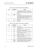
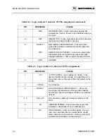
Table 4-14. Logic Analyzer Connector J20 Pin Assignments
PIN
MNEMONIC
SIGNAL
1 – 4
SPARE
No connection
5 – 8
GND
GROUND
9
MISO
MASTER-IN, SLAVE-OUT – Serial input to SPI in
master mode; serial output from SPI in slave mode.
10
MOSI
MASTER-OUT, SLAVE-IN – Serial output from SPI in
master mode; serial input to SPI in slave mode.
11
SCK
SPI SERIAL CLOCK – In master mode, the clock
signal from the SPI; in slave mode the clock signal to
the SPI.
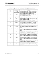
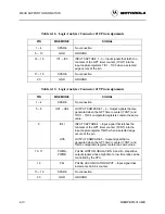
12
PCS0 /
SS
PERIPHERAL CHIP SELECT 0 – Active-low output
SPI peripheral chip select signal.
SLAVE SELECT – Bi-directional, active-low signal that
initiates serial transmission when SPI is in slave mode;
causes mode fault in master mode.
13 – 15
PCS1 – PCS3
PERIPHERAL CHIP SELECT 1 – 3 – Active-low
output SPI peripheral chip select signal.
16
RXD
RECEIVE DATA – RS-232C serial data input line.
17
TXD
TRANSMIT DATA – Serial data output line.
18
PCLK
AUXILIARY TIMER CLOCK INPUT – External input
clock source to the GPT.
19
SPARE
No connection
20
GND
GROUND


