background image


M68360QUADS-040 Hardware User’s Manual

Hardware Preparation and Installation


13


2.3.1  

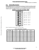
ADI Port Address Selection


The M68360QUADS-040 can have eight possible slave addresses set for its ADI port, enabling up to eight
M68360QUADS-040 boards to be connected to the same ADI board in the host computer. The selection
of the slave address is done by setting switches 6, 7 & 8 in the Dip-Switch. Switch 6 stands for the most-
significant bit of the address and switch 8 stands for the least-significant bit. If the switch is in the ’ON’ state,
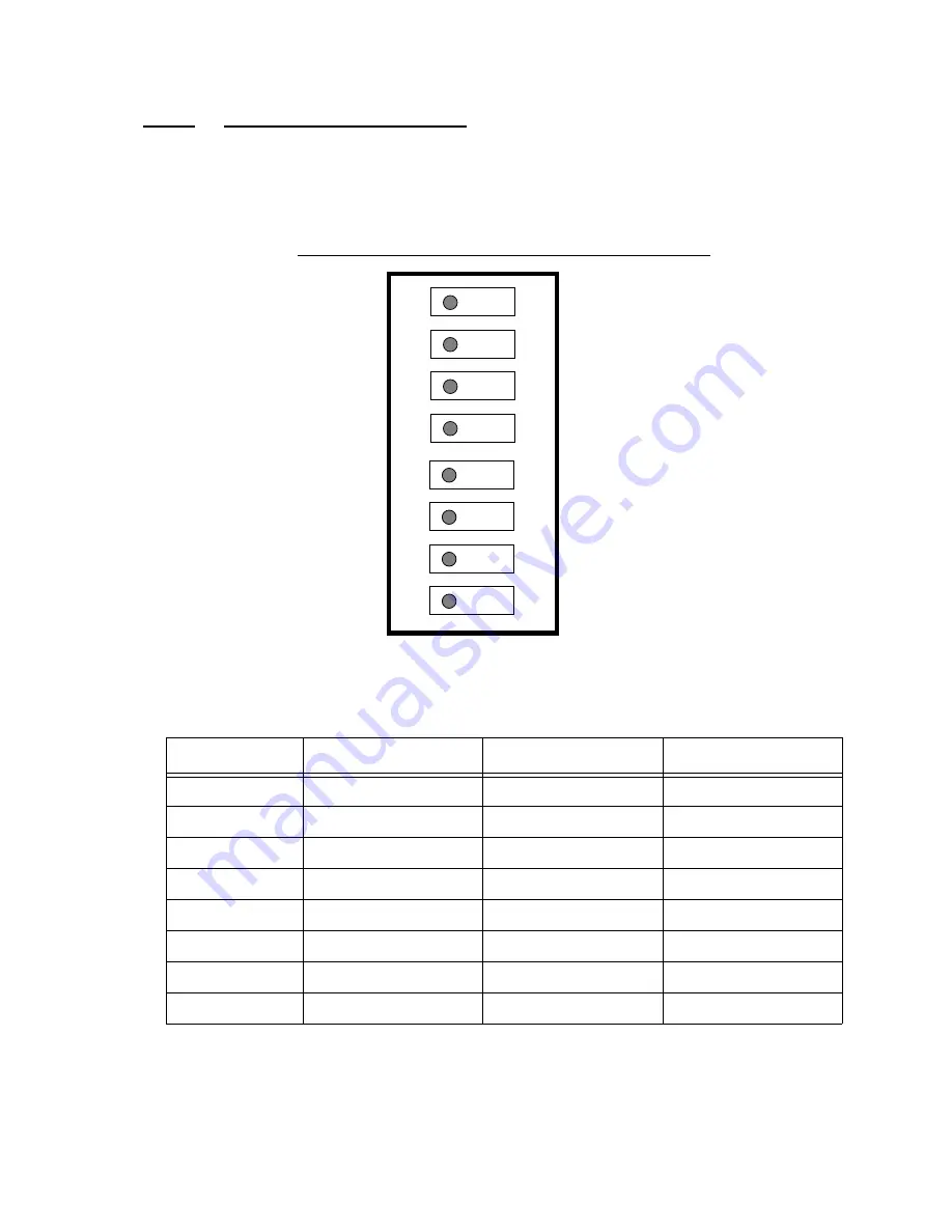
it stands for logical ’1’. In FIGURE 2-2 DSW1 is shown to be configured to address ’0’.


FIGURE 2-2   Configuration Dip-Switch - DSW1


Table 2-1 describes the switch settings for each slave address:


Table 2-1 ADI Address Selection


ADDRESS

Switch 6

Switch 7

Switch 8

0

OFF

OFF

OFF

1

OFF

OFF

ON

2

OFF

ON

OFF

3

OFF

ON

ON

4

ON

OFF

OFF

5

ON

OFF

ON

6

ON

ON

OFF

7

ON

ON

ON

DSW1

ON

5

6

7

8

1

2

3

4

SEL2: ON - ’1’, OFF ’0’

SEL1: ON - ’1’, OFF ’0’

SEL0: ON - ’1’, OFF ’0’

OPT2: ON - ’1’, OFF ’0’

OPT1: ON - ’1’, OFF ’0’

OPT0: ON - ’1’, OFF ’0’

CDIS~: ON - DISABLED

MDIS~: ON - DISABLED


F

re

e

sc

a

le

 S

e

m

ic

o

n

d

u

c

to

r,

 I


Freescale Semiconductor, Inc.

For More Information On This Product,

   Go to: www.freescale.com

n

c

.

..

Summary of Contents for M68360QUADS-040

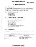
Page 1: ... MICROPROCESSOR MEMORY TECHNOLOGIES GROUP M68360QUADS 040 User s Manual ISSUE 1 0 DRAFT Thi d t t d ith F M k 4 0 4 Freescale Semiconductor I Freescale Semiconductor Inc For More Information On This Product Go to www freescale com nc ...

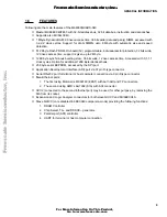
Page 2: ...NG INSTRUCTIONS 17 3 1 INTRODUCTION 17 3 2 CONTROLS AND INDICATORS 17 3 2 1 SOFT RESET Switch SW1 17 3 2 2 ABORT Switch SW2 17 3 2 3 HARD RESET Switches SW1 SW2 17 3 2 4 EEST Configuration Jumpers J1 to J6 17 3 2 4 1 TPEN Jumper J1 17 3 2 4 2 APORT Jumper J2 17 3 2 4 3 TPAPCE Jumper J3 17 3 2 4 4 TPSQEL Jumper J4 17 3 2 4 5 TPFULDL Jumper J5 18 3 2 4 6 LOOP Diagnostic Loopback Jumper J6 18 3 2 5 H...

Page 3: ...in Register 24 3 4 21 Port B Data Register 24 3 4 22 Port B Data Direction Register 25 3 4 23 Port B Pin Assignment Register 25 3 4 24 Port C Data Register 25 3 4 25 Port C Data Direction Register 25 3 4 26 Port C Pin Assignment Register 25 3 4 27 Port C Special Options Register 25 4 FUNCTIONAL DESCRIPTION 26 4 1 INTRODUCTION 26 4 2 Master MC68EC040 26 4 2 1 RESET for the 68EC040 the QUICC 26 4 2 ...

Page 4: ...Signals 44 5 2 7 Connector P7 Interconnect Signals 44 5 2 8 Connector P8 Interconnect Signals 44 5 2 9 Connector P9 Interconnect Signals 45 5 2 10 Connector P10 Interconnect Signals 47 5 2 11 Connector P11 Interconnect Signals 47 5 3 M68360QUADS 040 Parts List 47 A 1 INTRODUCTION 51 A 2 IBM PC XT AT to M68360QUADS 040 Interface 51 A 2 1 ADI Installation in IBM PC XT AT 51 A 3 SUN 4 to M68360QUADS ...

Page 5: ...r 35 FIGURE 4 4 Status Register 35 FIGURE 4 5 Ethernet AUI Port Connector 36 FIGURE 4 6 Ethernet Twisted Pair Port Connector 37 FIGURE A 1 Physical Location of jumper JG1 and JG2 52 FIGURE A 2 JG1 Configuration Options 52 FIGURE A 3 ADI board for SBus 53 FIGURE B 1 Host Computer ADI to M68360QUADS 040 Connection 56 FIGURE B 2 Host Write to M68360QUADS 040 57 FIGURE B 3 M68360QUADS 040 Write Cycle ...

Page 6: ...rconnect Signals 37 TABLE 5 2 Connector P2 Interconnect Signals 38 TABLE 5 3 Connector P3 Interconnect Signals 38 TABLE 5 4 Connector P8 Interconnect Signals 39 TABLE 5 5 Connector P5 Interconnect Signals 39 TABLE 5 6 Connector P6 Interconnect Signals 40 TABLE 5 7 Connector P7 Interconnect Signals 40 TABLE 5 8 Connector P8 Interconnect Signals 40 TABLE 5 9 Connector P9 Interconnect Signals 41 TABL...

Page 7: ... for the QUICC device ADI Application Development Interface UART Universal Asynchronous Receiver Transmitter SIMM Single In line Memory Module AUI Attachment Unit Interface SPI Serial Peripheral Interface NMI Non Maskable Interrupt EEST Enhanced Ethernet Serial Transceiver the MC68160 SIA Serial Interface Adapter the Am7992 TP Twisted Pair nsec nano second 1 4 SPECIFICATIONS The M68360QUADS 040 sp...

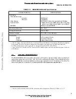
Page 8: ... timing between the QUICC the EC040 c Since A28 to A31 of the slave QUICC are used as Write Enable signals the on board addressing space is reduced to 256 MBytes 1 If no heat sink is attached to the 68EC040 maximum ambient temperature allowed 25 Mhz is 4 O C Addressing Total address range on board Off board Flash Memory Dynamic RAM EEPROM 256 MBytesc 4 GigaBytes 512 KByte 32 bits wide expandable t...

Page 9: ...8K Byte identical bank 256 byte serial EEPROM accessed by the SPI port Application Development Interface ADI port via 37 pin D type connector Serial RS 232 port for terminal or host computer connection via 9 pin Dtype connector Two Ethernet ports 1 The first using Motorola s MC68160 EEST with both AUI and TP connectors 2 The second using AMD s Am7992 SIA with AUI connector SCC2 connected to the se...

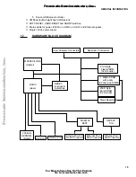
Page 10: ...DRAM 256 Byte EEPROM ADI Port RS 232 Port Expansion Connectors Logic Analyzer Connectors MC68EC LC040 master QUICC slave Ethernet Port EEST MC68160 512 KByte Flash PROM AUI Connector Ethernet Port T P RJ 45 Connector 32 bits wide Serial 36 bits wide SIMM with parity 256 K Byte Burst SRAM 36 bit wide Staus Register SIA AM7992 Ethernet Port AUI Connector RESET Interrupt Indications Freescale Semicon...

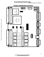
Page 11: ...PREPARATION To select the desired configuration and ensure proper operation of the M68360QUADS 040 board changes of the Dip Switch settings may be required before installation The location of the switches LEDs Dip Switches and connectors is illustrated in FIGURE 2 1 The board has been factory tested and is shipped with Dip Switch settings as described in the following paragraphs Parameters can be ...

Page 12: ...M U22 U33 U34 U35 U36 Dip Switch SW1 SW2 ABORT SOFT RESET MC68EC040 U24 U25 SLAVE QUICC MC68360 P2 P5 P4 Ethernet AUI SIA Ethernet TP P3 Ethernet AUI EEST DSW1 1 Flash Memory U18 U19 U20 U21 U27 U28 U29 U30 BURSTING SRAM P8 J7 J8 J9 J10 1 A 1 1 1 1 J1 J2 J3 J4 J5 J6 Freescale Semiconductor I Freescale Semiconductor Inc For More Information On This Product Go to www freescale com nc ...

Page 13: ...st significant bit If the switch is in the ON state it stands for logical 1 In FIGURE 2 2 DSW1 is shown to be configured to address 0 FIGURE 2 2 Configuration Dip Switch DSW1 Table 2 1 describes the switch settings for each slave address Table 2 1 ADI Address Selection ADDRESS Switch 6 Switch 7 Switch 8 0 OFF OFF OFF 1 OFF OFF ON 2 OFF ON OFF 3 OFF ON ON 4 ON OFF OFF 5 ON OFF ON 6 ON ON OFF 7 ON O...

Page 14: ...connected the QUICC s Parity Error line PERR is connected to the QUICC s level 5 interrupt request line IRQ5 to generate level 5 interrupt upon parity error occurrence When J8 is disconnected no parity error interrupt is generated J8 is disconnected at factory 2 3 5 Arbitration Configuration To allow for external master to be connected off board the arbitration scheme must be changed Jumper J9 con...

Page 15: ...S 040 requires 12 Vdc 1 A max power supply for the Ethernet AUI port The M68360QUADS 040 can work properly without the 12V power supply if the AUI port is not in use or if the AUI port is used with an AUI hub that does not require 12 V to be provided by the network termination equipment Connect the 12V power supply to connector P6 as shown below FIGURE 2 4 P6 12V Power Connector P6 is a 2 terminal...

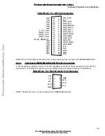
Page 16: ... shown in FIGURE 2 6 FIGURE 2 6 P2 RS 232 Serial Port Connector NOTE The RTS line pin 7 is not connected in the M68360QUADS 040 Gnd 20 INT_ACK 1 2 Gnd 21 Gnd 22 Gnd 23 Gnd 24 Gnd 25 12 v N C 26 HST_ACK 3 ADS_ALL 4 HOST_VCC ADS_RESET ADS_SEL2 ADS_SEL1 ADS_SEL0 5 6 7 8 27 HOST_VCC HOST_VCC Gnd Gnd HOST_ENABLE HOST_REQ ADS_REQ ADS_ACK ADS_INT HOST_BRK ADS_BRK 9 10 11 12 13 14 28 29 30 31 32 Gnd 33 PD...

Page 17: ...set all its configuration is lost and has to be re initialized 3 2 4 EEST Configuration Jumpers J1 to J6 The following jumpers J1 to J6 are used to determine the EEST operation modes according to the description below 3 2 4 1 TPEN Jumper J1 The TPEN Twisted Pair Enable jumper determines the interface type of the EEST ethernet port When in position along with J2 the EEST port uses the AUI interface...

Page 18: ...ata out of the data cache 3 2 6 Parity Error Interrupt Jumper J8 When J8 is positioned in place and parity is enabled occurrence of parity error causes a level 5 interrupt to the EC040 via the QUICC s interrupt controller When J8 is removed parity error interrupts are disabled 3 2 7 Bus Request Jumper J9 When J9 is in position the Bus Request BR Output of the EC040 is connected to the Bus Request ...

Page 19: ...D6 The red LED Ethernet TP Polarity indicator PLR lights if the wires connected to the receiver input of TP P4 port are reversed The LED is lit by the EEST and remains on when the EEST has automatically corrected for the reversed wires 3 2 17 Ethernet JABB Indicator LD1 The red LED Ethernet TP Jabber indicator JABB lights whenever a jabber condition is detected on the TP P4 port 3 2 18 POWER Indic...

Page 20: ...al b Connected to D0 D15 100 00 MMU Table Searchb Code All 101 0X Supervisor Data All 110 00 Supervisor Program All 111 00 Supervisor CPU QUICC s MBAR register 111 11 Supervisor CPU QUICC during interrupt acknowledge cycle TABLE 3 2 M68360QUADS 040 Main Memory Map ADDESS RANGE Accessed Device Data Size NOTES 00000000 001FFFFF Flash PROM 32 2 00200000 003BFFFF Empty Space 003C0000 003CFFFF Bursting...

Page 21: ... control register CLKOCR controls the operation of the CLKO 1 2 pins This register must be initialized to 03 after reset to enable CLKO2 and disable CLKO1 3 4 4 PLL Control Register The PLL control register PLLCR controls the operation of the PLL There is no need to program the PLLCR after hard reset because the configuration of the MODCK 0 1 pins on the QUADS determines its value It is recommende...

Page 22: ...rites Same length 040 SRAM reads writes Parity is disabled The CS RAS lines of the slave QUICC will not assert when accessing the CPU space Internal address multiplexing for the DRAM is disabled 3 4 8 Base Register 0 and Option Register 0 Base register 0 BR0 and Option register 0 OR0 control the operation of CS0 pin of the slave QUICC which serves as the Flash Prom chip select BR0 is initialized t...

Page 23: ...200 type BR2 must be initialized to 800021 OR2 initialization depends also of the DRAM SIMM type installed on the M68360QUADS 040 as to the following For MCM36256 or MCM36512 types For 100 nsec access time 3FF00001 For 80 nsec or 70 nsec access time 2FF00001 For 60 nsec access time 1FF00001 For MCM36100 or MCM36200 types For 100 nsec access time 3FC00021 For 80 nsec or 70 nsec access time 2FC00001...

Page 24: ...for that pin is driven onto the pin On the M68360QUADS 040 port A is used for serial channels as well as for ADI parallel port PADAT must be initialized to 3F00 before configuring the other port registers 3 4 18 Port A Data Direction Register The port A data direction register PADIR has different functions according to the configuration of the port pins If a pin is a general purpose I O pin the va...

Page 25: ... capability The Port C data register PCDAT can be read to check the data at the pin If a port pin is configured as general purpose output pin the value in the PCDAT for that pin is driven onto the pin It is recommended to initialize PCDAT to 000 before configuring the other port registers 3 4 25 Port C Data Direction Register The port C data direction register PCDIR has different functions accordi...

Page 26: ... types of reset regarding their source and consequence available on the M68360QUADS 040 board 1 QUICC Generated Reset These types of reset are generated internally by the QUICC and include Power up Software Watch Dog Double Bus Fault reset is not supported when the QUICC is in EC040 companion mode 2 SOFT Reset may be caused by either depressing the SOFT RESET push button or when the ADI port s sof...

Page 27: ...e desired memory space2 to be shielded BKPTO will be asserted on the relevant access to that space and avoid redundant caching 4 3 Interrupts on the M68360QUADS 040 In slave mode including 68EC040 companion the QUICC serves as an interrupt encoder for the master processor It integrates all internal and external interrupt sources and encodes them to IOUT 0 2 to be connected to standard 68000 IPL li...

Page 28: ...host computer of either HOST_REQ or HOST_ACK signals when the board is selected to generate a level 2 maskable interrupt to the EC040 4 4 Bus Arbitration When a QUICC is configured in 68EC040 companion mode its arbiter lines do not change function and the QUICC remainsbus arbiter rather than a requester as in other slave modes The 68EC040 arbitration lines are connected gluelessly to those of the ...

Page 29: ...the address in the BKAR and to the access attributes in the BKCR If there is a match the BKPTO signal is asserted by the QUICC Since TS is asserted only at the beginning of the cycle no address comparison is done for the rest of the access burst access The BKPTO of the slave QUICC is wired via a jumper to generate a non maskable interrupt on level 7 If the EC040 performs a breakpoint instruction t...

Page 30: ...fered U38 and distributed to all board consumers 4 7 Flash PROM The Flash PROM on the M68360QUADS 040 is constructed of four Am29F010 12 devices providing a total of 512 KBytes The Am29F010 is a 5 V programmable with 8 sectors protection capability 120 nsec access time 128 KByte device accessed with 3 wait states 25 Mhz system clock An option is made to use bigger Flash PROMs up to the Am29F040 Th...

Page 31: ...quire using RAS1 and RAS2 signals of the slave QUICC if they are organized as two memory banks After hard power up reset the status register is read to detect the kind of dram SIMM inserted in order to initialize the CS registers with the correct data regarding the dram s size and delay The DRAM is controlled by the slave QUICC device using its DRAM controller function for normal accesses burst mo...

Page 32: ...lel link from the M68360QUADS 040 to various host computers This port is connected via a 37 line cable to a special board called ADI Application Development Interface installed in the host computer Two versions of the ADI board are available to support connection to IBM PC XT AT and SUN 4 SPARC stations It is possible to connect the M68360QUADS 040 board to these computers provided that the approp...

Page 33: ... QUADS 040 should be able to work properly with existing ADS boards such as the M68302ADS In the list below the directions I O and I O are relative to the M68360QUADS 040 board I E I means input to the M68360QUADS 040 NOTE Since the ADI was originated for the DSP56001ADS some of its signals throughout the boards it was used with were designated with the prefix ADS This convention is kept with this...

Page 34: ...he ADS_REQ signal HOST_BRK O This open collector signal generates an interrupt to the host This signal is common to all M68360QUADS 040 boards that are connected to the same ADI ADS_INT O This line is polled by the host computer during its interrupt acknowledge cycle to determine which M68360QUADS 040 board has generated the interrupt INT_ACK I This line is asserted by the host at the end of its i...

Page 35: ... an input register for ADI interface signals FIGURE 4 4 Status Register 4 11 5 1 Status Register Bits Description DTR When active 0 indicates that a terminal is connected to the serial port H_NMI When active 0 indicates that the last level 7 interrupt NMI was generated from the host via the ADI port INACK When active 0 indicates that a Host Interrupt Acknowledge cycle is in progress ADSSEL When ac...

Page 36: ...equire external glue logic The second Ethernet port is implemented by connecting SCC2 to AMD s SIA Am7992 device In this case however only AUI port is implemented via P5 To support other uses of SCC2 it s signals are available also at the expansion connectors and the SIA U4 is mounted on a socket That way the SIA can be removed freeing SCC2 signals for other use via the expansion connector P11 4 1...

Page 37: ... 1 2 and 3 of port B and by a general purpose output pin pin 0 of port B The SPI port operates in master mode The serial EEPROM serves as non volatile memory on the M68360QUADS 040 and may be used to store software parameters to be protected from power downs 4 11 8 Slave QUICC General Purpose I O Pins The slave QUICC has three ports A B and C whose pins can be individually configured by software t...

Page 38: ...ted to The expansion connector P11 and may be utilized for user s applications 8 EEST TCLK This pin is connected to the transmit clock output of the EEST It is configured as the transmit clock of SCC1 in the slave QUICC 9 EEST RCLK This pin is connected to the receive clock output of the EEST It is configured as the receive clock of SCC1 in the slave QUICC 10 SIA TCLK This pin is connected to the ...

Page 39: ... PD0 through the data bus transceiver U13 and it is configured as I O pin 11 ADI Data 1 This pin is connected to the ADI port signal PD1 through the data bus transceiver U13 and it is configured as I O pin 12 ADI Data 2 This pin is connected to the ADI port signal PD2 through the data bus transceiver U13 and it is configured as I O pin 13 ADI Data 3 This pin is connected to the ADI port signal PD3...

Page 40: ... QUICC 2 3 PC2 PC3 These pins are connected to the expansion connector P11 and may be used by user s applications 4 EEST CLSN This pin is connected to the CLSN output of the EEST It is configured as the CTS signal of SCC1 in the slave QUICC 5 EEST RENA This pin is connected to the RENA output of the EEST It is configured as the CD signal of SCC1 in the slave QUICC 6 SIA CLSN This pin is connected ...

Page 41: ...type connector It is the ADI port of the M68360QUADS 040 TABLE 5 1 describes the P1 connector signals 1 Connector P10 has identical pinout to P8 2 Connector P11 has identical pinout to P9 TABLE 5 1 Connector P1 Interconnect Signals Pin No Signal Name Description 1 INT_ACK Interrupt Acknowledge input signal from the host 2 Not connected 3 HST_ACK Host Acknowledge input signal from the host 4 ADS_AL...

Page 42: ...ABLE HOST Enable input signal from the host 31 33 GND Ground signal of the M68360QUADS 040 34 PD0 Bit 0 of the ADI port data bus 35 PD2 Bit 2 of the ADI port data bus 36 PD4 Bit 4 of the ADI port data bus 37 PD6 Bit 6 of the ADI port data bus TABLE 5 2 Connector P2 Interconnect Signals Pin No Signal Name Description 1 CD Carrier Detect output from the M68360QUADS 040 2 TX Transmit Data output from...

Page 43: ... signal of the M68360QUADS 040 12 ARX Receive Data negative input to the M68360QUADS 040 13 VPP 12V power supply from the M68360QUADS 040 14 GND Ground signal of the M68360QUADS 040 15 Not connected TABLE 5 4 Connector P8 Interconnect Signals Pin No Signal Name Description 1 TPTX Twisted Pair Transmit Data positive output from the M68360QUADS 040 2 TPTX Twisted Pair Transmit Data negative output f...

Page 44: ...detect negative input to the M68360QUADS 040 10 ATX Transmit Data negative output from the M68360QUADS 040 11 GND Ground signal of the M68360QUADS 040 12 ARX Receive Data negative input to the M68360QUADS 040 13 VPP 12V power supply from the M68360QUADS 040 14 GND Ground signal of the M68360QUADS 040 15 Not connected TABLE 5 6 Connector P6 Interconnect Signals Pin No Signal Name Description 1 VCC ...

Page 45: ...d C16 LOCK EC040 Locked RMW Cycle indicator C17 DD2 Quicc s RAS Double Drive 2 C18 TBI EC040 s Transfer Burst Inhibit C19 TA EC040 s Transfer Acknowledge C20 TEA EC040 s Transfer Error Acknowledge C21 VCC Board s VCC plane C22 RSTH Hard reset pin of the QUICC C23 RSTS Soft reset pin of the QUICC C24 PERR Parity error pin of the QUICC C25 VCC Board s VCC plane C26 TS EC040 s Transfer Start C27 WE0 ...

Page 46: ...icc s Port B s Parallel I O lines 4 9 B11 TIP EC040 s Transfer In Progress B12 BR040 EC040 s Bus Request B13 BG040 EC040 s Bus Grant B14 B17 PST0 PST3 EC040 s Processor Status 0 3 B18 B19 SC0 SC1 EC040 s Snoop Control 0 1 B20 GND Board s Ground B21 S_TENA SIA s Transmit Enable Input B22 B23 PC2 PC3 Quicc s Port C Parallel I O lines 2 3 B24 B25 GND Board s Ground B26 S_CLSN SIA s Collision Indicato...

Page 47: ... C17 MI EC040 s Memory Inhibit output C18 CIOUT EC040 Cache Inhibit Out C19 IPEND EC040 Interrupt Pending output C20 CDIS EC040 s Cache Disable input C21 BKPTO Quicc s BreakPoint Output C22 RSTH Quicc s Hard Reset signal C23 RSTS Quicc s Soft Reset signal C24 BADD3 Quicc s Burst Address line 3 C25 MDIS a LC040 s Memory Management Unit Disable Input C26 BADD2 Quicc s Burst Address line 2 C27 DD1 Qu...

Page 48: ...in D type female P3 P5 Connector 15 pin D type female P4 Connector 8 pin RJ 45 P6 Power connector 3 pin with plug 5v power supply P7 Power connector 2 pin with plug 12v power supply P8 P9 Connector 96 pin DIN male straight Logic analyzer P10 P11 Connector 96 pin DIN female 900 Compatible wire wrap connectors are supplied with the M68360QUADS 040 Expansion R1 R3 R12 R14 R18 R21 Resistor 39 1 Ω SMD ...

Page 49: ...SMD U10 U11 I C PAL20RA10 20 DIP socket mounted U12 I C PAL22V10 25 DIP socket mounted U13 I C 74LS245 SMD U14 I C MCM2814 DIP U15 I C 74LS85 SMD U16 U38 I C 74ACT86 SMD U17 U26 U31 I C 74F157 SMD U18 U21 I C Am29F010 12 SMD socket mounted U22 I C MCM36256 DRAM SIMM SIMM socket mounted U23 I C PAL22V10 15 DIP socket mounted U24 MC68EC040FE33 CQFP U25 MC68360 QUICC PGA socket mounted U27 U30 U33 U3...

Page 50: ...M68360QUADS 040 Hardware User s Manual SUPPORT INFORMATION 50 Freescale Semiconductor I Freescale Semiconductor Inc For More Information On This Product Go to www freescale com nc ...

Page 51: ...PUTER TURN THE POWER OFF AND REMOVE THE POWER CORD A 2 1 ADI Installation in IBM PC XT AT Refer to the appropriate Installation and Setup manual of the IBM PC XT AT computer for instructions on removing the computer cover The ADI board address block should be configured at a free I O address space in the computer The address must be unique and it must not fall within the address range of another c...

Page 52: ...out of the way lower the board until its connectors are aligned with the computer expansion slot connectors Using evenly distributed pressure press the ADI board straight down until it seats in the expansion slot Secure the ADI board to the computer chassis using the bracket retaining screw Refer to the computer Installation and Setup manual for instructions on reinstalling the computer cover A 3 ...

Page 53: ...ame bin su Password mypasswd hostname usr etc halt wait for the following messages Syncing file systems done Halted Program Terminated Type b boot c continue n new command mode When these messages appear you can safely turn off the power to the system unit 2 Open the system unit Be sure to attach a grounding strap to your wrist and to the metal casing of the power supply Follow the instructions su...

Page 54: ...nd gently press the corners of the board to seat the connector firmly 6 Close the system unit 7 Connect the 37 pin interface flat cable to the ADI board and secure 8 Turn power on to the system unit and check for proper operation Freescale Semiconductor I Freescale Semiconductor Inc For More Information On This Product Go to www freescale com nc ...

Page 55: ...an write a byte to the host computer The M68360QUADS 040 can interrupt the host computer The host computer can interrupt the M68360QUADS 040 interrupt level 7 The host computer can reset soft or hard the M68360QUADS 040 If more than one M68360QUADS 040 is connected to the same ADI board the host computer can perform the following operations simultaneously on all M68360QUADS 040 boards Abort all bo...

Page 56: ...UADS 040 is as follows 1 The Host selects the M68360QUADS 040 board by putting the board s address on the ADS_SEL 0 2 signals 2 The Host places a data byte in the data bus latch buffer is in high impedance state 3 The Host asserts the HOST_REQ signal the data buffer is enabled data appears on the bus 4 The M68360QUADS 040 detects the HOST_REQ signal and reads the data byte 5 The M68360QUADS 040 as...

Page 57: ...bled and asserts the ADS_REQ signal the ADS_REQ signal will not appear on the port until the board is selected by the Host 2 The Host polls each M68360QUADS 040 address and detects the ADS_REQ signal from the requesting board The Host asserts the HST_ACK signal in response which enables the data buffer in the M68360QUADS 040 3 The M68360QUADS 040 negates the ADS_REQ signal The data appears on the ...

Page 58: ...ted by the Host 2 The Host detects the HOST_BRK signal and polls each M68360QUADS 040 address to determine the interrupting board 3 The Host asserts the HST_ACK signal enabling the data buffer in the M68360QUADS 040 4 The Host reads the service request code on the data bus 5 The Host negates the HST_ACK signal 6 The Host asserts the INT_ACK signal which resets the HOST_BRK latch in the M68360QUADS...

Page 59: ...r hard reset or soft reset on the M68360QUADS 040 Soft reset is done by selecting the address of the required board and asserting the ADS_RESET signal for more than 26 microseconds Hard reset is done by selecting the address of the required board asserting INT_ACK signal and asserting the ADS_RESET signal for more than 26 microseconds B 3 6 Addressing All M68360QUADS 040 The Host can reset or inte...

Page 60: ...ic and future support for MC68040 buffers configuration via IPL RUN040 drives the run040 led when TIP is active low RUNDM drives the rundma led when AS is active low HLT drives the halt led according to the state of PST 0 3 H_NMI serves as a FF for the host generated level 7 interrupt H_BRK_ is a simulated o c output for the ADI s host break OE of which is driven by H_BRK EQUATIONS RUN040 VCC RUN0...

Page 61: ... PILOT 0 DATE 8 8 93 CHIP RSTABR PAL20RA10 This pal is used as a reset and abort generator for the QUICC040EVB DEB1 serves as a debouncer for the reset push button and DEB2 serves a debouncer for the abort p b IRQ7 which is the logical sum of all events causing level 7 interrupt i e abort push button breakpoint and host nmi drives the OE of IRQ7 to simulate open collector ABORT was removed since i...

Page 62: ... are depressed P B SOFT reset HOST hard and soft reset P U reset and software watch dog reset RSTI is separated from RSTH_ in order of supporting soft reset as well PL RST1 RST2 ABR1 ABR2 H_RSTH H_RSTS RSTO CS5 H_NMI BKPTO GND 1 2 3 4 5 6 7 8 9 10 11 12 OE RSTI DEB2 DEB1 ABRT RSTS RSTH BKINT IRQ7 RSTS_ RSTH_ VCC 13 14 15 16 17 18 19 20 21 22 23 24 EQUATIONS IRQ7 ABRT abort p b FF H_NMI host nmi BK...

Page 63: ...reset DEB1 DEB2 BOTH push buttons depressed RSTH TRST VCC RSTH RSTF VCC bypass RSTH SETF VCC BKINT CLKF BKPTO falling edge of BKPTO BKINT VCC active low BKINT TRST VCC BKINT RSTF CS5 reset the FF 1 BKINT SETF GND RSTI RSTH_ Quicc generated resets HOST hard reset DEB1 P B hard soft reset H_RSTS HOST soft reset RSTI TRST VCC RSTI RSTF VCC bypass RSTI SETF VCC RSTS_ VCC active low RSTS_ TRST RSTS RST...

Page 64: ...9 20 21 22 23 VCC GLOBAL 24 THE 25 TH PIN This pal serves as an ADI controller for the M68360QUADS 040 H_RSTS generates soft reset for the evb H_RSTH generates hard reset for the evb CK_NMI generates the level 7 interrupt BKCLR resets the host break FF ADI_RD open the strobes buffer towards the ADI ADI_G enables the data buffer ADI_AC generates interrupt upon HOST request or acknowledge ADIDIR con...

Page 65: ...IR HSTEN ADS_G HSVCC ADSSEL HSACK host read only C 4 U23 Core Disable Logic TITLE DISCPU PATTERN dis_bug pds Revision PILOT 0 DATE 9 8 93 This pal is meant to fix the core disable problem in the quicc It contains a 6 bit synchronous counter which starts counting after RESETH_ is asserted During the first 64 clocks since RESETH_ is asserted CONF2 is held at 1 to allow reset of the CORE On the next ...

Page 66: ...RESETH GND I1 I2 I3 I4 I5 I6 I7 I8 I9 I10 I11 12 NC Q5 Q4 Q3 Q2 Q1 Q0 CONF2 D_RST DS_RST S_RST VCC I13 O14 O15 O16 O17 O18 O19 O20 O21 O22 O23 24 GLOBAL EQUATIONS S_RST RESETH Sync RESETH S_RST TRST VCC DS_RST S_RST Double sync RESETH DS_RST TRST VCC D_RST S_RST DS_RST Identifying RESETH falling edge to synchronously reset the counter Q0 Q0 D_RST CIN Counter LSB Q0 D_RST CIN Q0 TRST VCC Q1 Q1 Q0 D...

Page 67: ... D_RST CIN Q4 Q2 D_RST CIN Q4 Q1 D_RST CIN Q4 Q0 D_RST CIN Q4 Q3 Q2 Q1 Q0 D_RST CIN Q4 D_RST CIN Q4 TRST VCC Q5 Q5 Q4 D_RST CIN Counter MSB Q5 Q3 D_RST CIN Q5 Q2 D_RST CIN Q5 Q1 D_RST CIN Q5 Q0 D_RST CIN Q5 Q4 Q3 Q2 Q1 Q0 D_RST CIN Q5 D_RST CIN Q5 TRST VCC CONF2 Q1 Q2 Q3 Q4 Q5 End of count CONF2 TRST RESETH Tristated after RESETH rising edge Freescale Semiconductor I Freescale Semiconductor Inc Fo...

Page 68: ... TS BAA 1 2 are active low Burst Address Advance for the srams BAA should be driven to the srams only during burst access and in burst write cycle one clock later than in burst read SAS is a one clock delayed AS CLK CS3 TS TIP AS SIZ0 SIZ1 TA R_W GND 1 2 3 4 5 6 7 8 9 10 OE CS4 NC SAS BAA2 TSC BAA1 SRMG2 SRMG1 VCC 11 12 13 14 15 16 17 18 19 20 EQUATIONS SRMG1 CS3 R_W SRMG1 TRST VCC SRMG2 CS4 R_W S...

Page 69: ...burst write BAA should be asserted one clock later BAA1 CS3 BAA2 SIZ1 SIZ0 TSC CS4 R_W TA TIP burst read SIZ1 SIZ0 TSC CS4 R_W TA TIP burst write BAA should be asserted one clock later BAA2 CS4 SAS AS CS4 TRST GND input Freescale Semiconductor I Freescale Semiconductor Inc For More Information On This Product Go to www freescale com nc ...

Page 70: ...Freescale Semiconductor I Freescale Semiconductor Inc For More Information On This Product Go to www freescale com nc ...

Page 71: ...Freescale Semiconductor I Freescale Semiconductor Inc For More Information On This Product Go to www freescale com nc ...

Page 72: ...Freescale Semiconductor I Freescale Semiconductor Inc For More Information On This Product Go to www freescale com nc ...

Page 73: ...Freescale Semiconductor I Freescale Semiconductor Inc For More Information On This Product Go to www freescale com nc ...

Page 74: ...Freescale Semiconductor I Freescale Semiconductor Inc For More Information On This Product Go to www freescale com nc ...

Page 75: ...Freescale Semiconductor I Freescale Semiconductor Inc For More Information On This Product Go to www freescale com nc ...

Page 76: ...Freescale Semiconductor I Freescale Semiconductor Inc For More Information On This Product Go to www freescale com nc ...

Page 77: ...Freescale Semiconductor I Freescale Semiconductor Inc For More Information On This Product Go to www freescale com nc ...

Page 78: ...Freescale Semiconductor I Freescale Semiconductor Inc For More Information On This Product Go to www freescale com nc ...

Page 79: ...Freescale Semiconductor I Freescale Semiconductor Inc For More Information On This Product Go to www freescale com nc ...

Page 80: ...Freescale Semiconductor I Freescale Semiconductor Inc For More Information On This Product Go to www freescale com nc ...

Page 81: ...Freescale Semiconductor I Freescale Semiconductor Inc For More Information On This Product Go to www freescale com nc ...

Page 82: ...Freescale Semiconductor I Freescale Semiconductor Inc For More Information On This Product Go to www freescale com nc ...

Page 83: ...Freescale Semiconductor I Freescale Semiconductor Inc For More Information On This Product Go to www freescale com nc ...

Page 84: ...Freescale Semiconductor I Freescale Semiconductor Inc For More Information On This Product Go to www freescale com nc ...

Page 85: ...Freescale Semiconductor I Freescale Semiconductor Inc For More Information On This Product Go to www freescale com nc ...

Page 86: ...Freescale Semiconductor I Freescale Semiconductor Inc For More Information On This Product Go to www freescale com nc ...

Reviews: