3-6
Theory of Operation
3.5.2
Antenna Switch
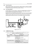
The antenna switch circuit consists of two pin diodes (D3521 and D3551), a pi network (C3531,
L3551, C3550), and two current limiting resistors (R3572-3). In the transmit mode, pin 32 of PCIC
U3502 goes high which applies a B+ source to the antenna switch circuit to bias the diodes "on". The
shunt diode (D3551) shorts out the receiver port and the pi network. This operates as a quarter wave
transmission line to transform the low impedance of the shunt diode to a high impedance at the input
of the harmonic filter. In the receive mode, the diodes are both off, creating a low attenuation path
between the antenna and receiver ports via L3551.
3.5.3
Harmonic Filter
The harmonic filter consists of components C3531-2, C3535-6, and L3531-2. The harmonic filter is a
modified Zolotarev design optimized for efficiency of the power module. This type of filter has the
advantage that it can give a greater attenuation in the stop-band for a given ripple level. The harmonic
filter insertion loss is typically less than 1.2 dB.
3.5.4
Antenna Matching Network
Because the 200 MHz antenna is a 50-ohm design, no matching circuitry is required between the
harmonic filter output and the 50-ohm SMA-style antenna connector (J3501).
3.5.5
Power Control Integrated Circuit (PCIC)
The transmitter uses the PCIC (U3502) to regulate the power output of the radio. The current drain of
the final device Q3501 is measured as the voltage drop across series resistor R3519. This voltage is
then fed back to the automatic level control (ALC) within the PCIC to regulate the output power of the
transmitter. The PCIC contains internal digital to analog converters (DACs) that provide a
programmable control loop reference voltage. The PCIC internal resistors, integrators, and external
capacitors (C3562-3 and C3565) control the transmitter rise and fall times to reduce the power
splatter into adjacent channels.
3.5.6
Temperature Cut Back Circuit
Temperature sensor U3503 and associated components are part of a temperature cutback circuit.
This circuit senses the printed circuit board temperature around the transmitter circuits and outputs a
DC voltage to the PCIC. If the DC voltage produced exceeds the set threshold of the PCIC, the
transmitter output power decreases to reduce the transmitter temperature.
3.6
200 MHz Receiver
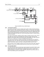
The 200 MHz receiver design is separated into two blocks, the front end and the back end. The overall
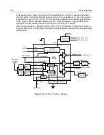
block diagram of the receiver is shown in Figure 3-6. Detailed descriptions of these stages are
contained in the paragraphs that follow.
Summary of Contents for HT1250-LS+
Page 10: ...viii ...
Page 12: ...x Product Safety and RF Exposure Compliance ...
Page 16: ...1 4 Introduction ...
Page 58: ...4 22 Maintenance ...
Page 64: ...5 6 Schematic Diagrams Overlays and Parts Lists ...


