6871620L01-C
May 28, 2008
Theory of Operation:
Transceiver Section
3-7
3.1.3
Transmitter
The transmitter takes modulated RF from the FGU and amplifies it to the radio's rated output power
to produce the modulated transmitter carrier at the antenna.
NOTE:
Table 8.1, “List of Schematics and Boards Overlays,” on page 8-1
for a listing of
transmitter-related schematics that will aid in the following discussion.
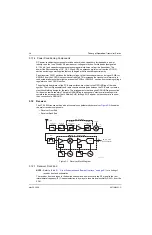
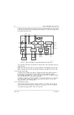
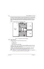
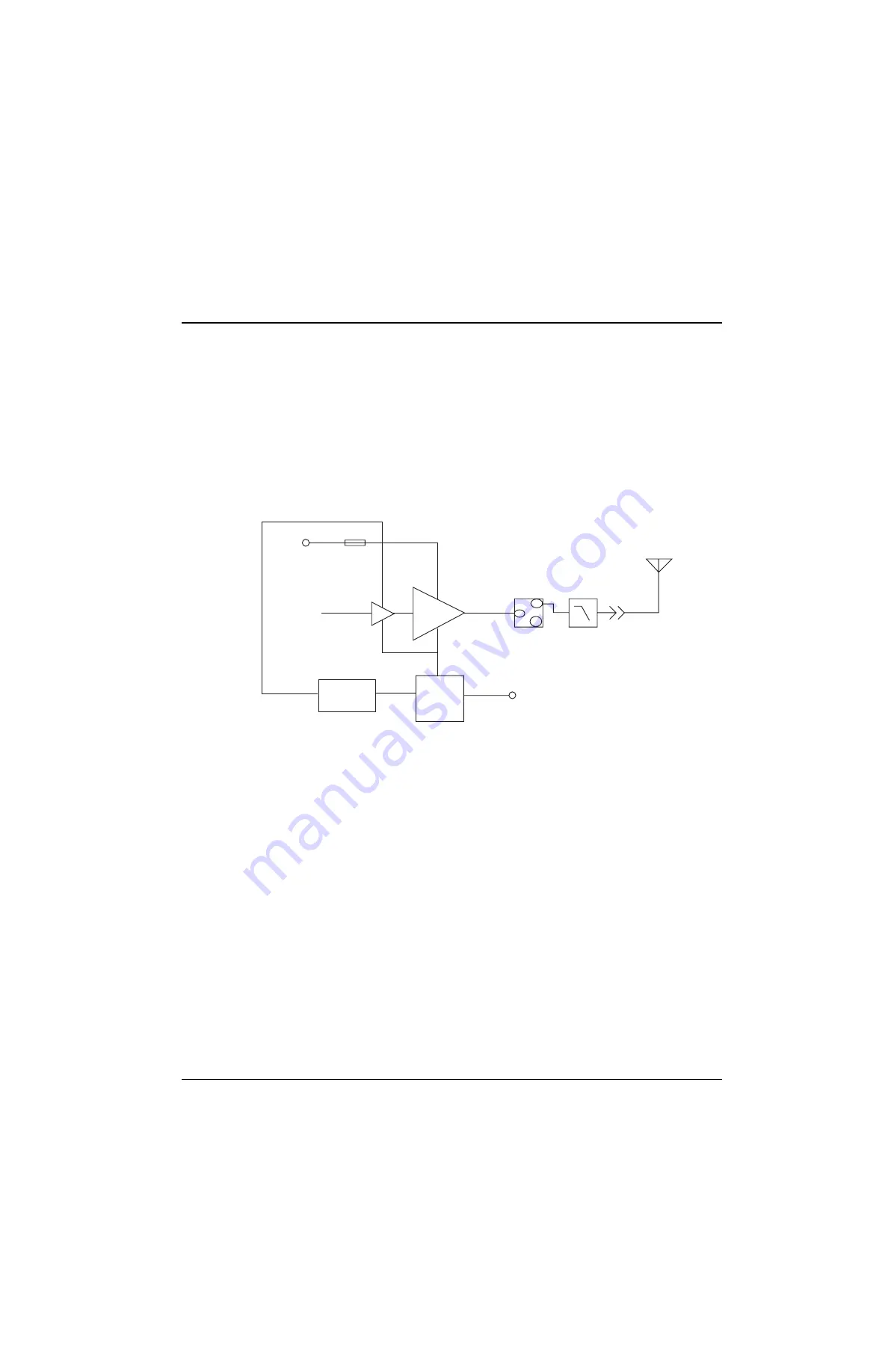
The transmitter (
) consists of an RF driver IC that receives its input signal from the
voltage-controlled oscillator (VCO) and a high-power output transistor. Transmitter power is
controlled by a power-control IC (PCIC) that senses the total current drawn by the transmit gain
stages and adjusts PA control voltages to maintain a constant power level. The signal passes
through an antenna switch and harmonic filter to the antenna.
Figure 3-5. Transmitter Block Diagram
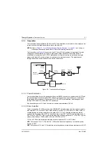
3.1.3.1 Power Distribution
To minimize voltage drop to the power amplifiers, net RAWB+ connects to power module Q107 and
the second stage of driver amplifier U102 through components having minimal series resistance –
ferrite beads and chokes only. During receive, no RF or DC bias is applied, and leakage current
through U102 and Q107 is less than 100 microamps.
At a transmitter power of 2 Watts, the radio consumes approximately 1100 mA.
3.1.3.2 Driver Amplifier
The driver amplifier IC (U102) contains two LDMOS FET amplifier stages and two internal resistor
bias networks. Pin 16 is the RF input. Modulated RF from the FGU, at a level of +3 dBm ±2 dB, is
coupled through a blocking capacitor to the gate of FET-1. An LC interstage matching network
connects the first stage output VD1 to the second stage input G2. The RF output from the drain of
FET-2 is pin 6 (RFOUT1). Gain control is provided by a voltage applied to pin 1 (VCNTRL). Typical
output power is about +26 dBm (400 mW) with VCNTRL at 4.5 V.
L101 and C102 are the interstage matching network; capacitor C111 is a DC block.
VHF:
Components C112–C115 and L103–L104 match the output impedance to maximize power
transfer to Q107.
UHF:
Components C114 and L113 match the output impedance to maximize power transfer to Q107.
RAWB+
Sense
Resistor
Driver
Amplifier
Modulated
RF from FGU
Power
Amplifier
Antenna
Switch
Harmonic
Filter
INT
Secondary
Cutback
PCIC
RFIN
RAWB+
Antenna
Summary of Contents for ASTRO XTSTM 4000
Page 1: ...COLOR CHORDS 7 ASTRO XTSTM 4000 Portable Radio Detailed Service Manual ...
Page 2: ......
Page 16: ...May 28 2008 6871620L01 C xiv Commercial Warranty Notes ...
Page 22: ...May 28 2008 6871620L01 C 1 6 Introduction Notes ...
Page 26: ...May 28 2008 6871620L01 C 2 4 Radio Power Notes ...
Page 56: ...May 28 2008 6871620L01 C 3 30 Theory of Operation Notes ...
Page 100: ...May 28 2008 6871620L01 C 6 8 Troubleshooting Waveforms Notes ...
Page 194: ...May 28 2008 6871620L01 C B 2 Motorola Service Centers Notes ...
Page 204: ...May 28 2008 6871620L01 C Glossary 10 Glossary Notes ...
Page 209: ......

