Fabric Interface Controller
UG0331 User Guide Revision 15.0
766
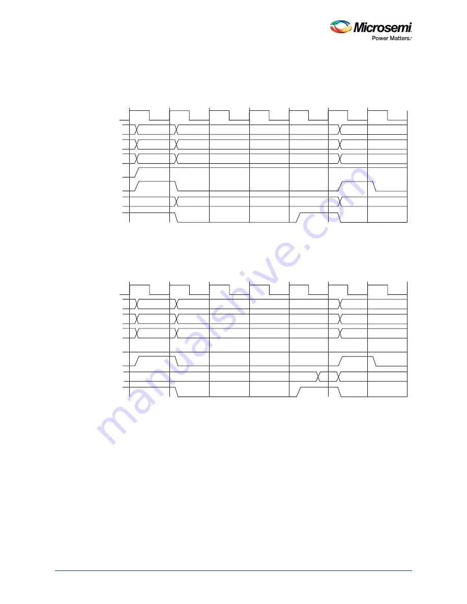
The following diagram shows the AHB-Lite bus signals from the fabric master to the fabric interface
controller for write transactions in Synchronous Pipelined mode. Generation of pipelined requests
depends on the efficiency of the master in the fabric to generate it.
Figure 335 •
AHB-Lite Bus Signals from Fabric Master to FIC for a Write Transaction in Synchronous Pipelined
Mode
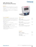
The following diagram shows the AHB-Lite bus signals from the fabric master to the fabric interface
controller for read transactions in Synchronous Pipelined mode. Generation of pipelined requests
depends on the efficiency of the master in the fabric to generate it.
Figure 336 •
AHB-Lite Bus Signals from Fabric Master to FIC for a Read Transaction in Synchronous Pipelined
Mode
Note:
When the Fabric master accesses MSS slave through the FIC_1 AHB-Lite slave interface, the AHB-to-
AHB bridge inserts a one-cycle delay in each direction. Since these timing diagrams are at FIC interface
level, the delay cannot be noticed.
24.5
Implementation Considerations
In AHB mode, the user may perform byte, half word and word accesses from the fabric to MSS.
However, in APB16 mode, the user can only cause a word access to occur to an MSS slave. This is done
by two accesses over the APB16, one of which is to write a 16-bit holding register (in the case of writes)
or to read a 16-bit holding register in the case of reads.
24.6
Fabric Interface Clocks
The fabric alignment clock controller (FACC) block in the MSS DDR clock controller is responsible for the
alignment of fabric related clocks. The FACC is interfaced with MSS PLLs (MPLLs) in order to generate
the various aligned clocks required by the MSS peripherals and the DDR controller in the MSS (MDDR).
The lowest frequency clock, of the aligned clocks being used within the fabric, is fed to the MSS DDR
clock controller and is referred to as CLK_BASE. CLK_BASE is internally multiplied and divided within
T1
T2
T3
T4
T5
T6
T7
T8
A
A + 4
00
00
10
10
10
10
FIC_X_AHB_S_HCLK
FIC_X_AHB_S_HADDR[31:0]
FIC_X_AHB_S_HTRANS
FIC_X_AHB_S_HSIZE
FIC_X_AHB_S_HWRITE
FIC_X_AHB_S_HSEL
FIC_X_AHB_S_HWDATA[31:0]
FIC_X_AHB_S_HREADY
Data (A)
Data (A+4)
T1
T2
T3
T4
T5
T6
T7
T8
A
A + 4
00
00
10
10
10
10
FIC_X_AHB_S_HCLK
FIC_X_AHB_S_HADDR[31:0]
FIC_X_AHB_S_HTRANS
FIC_X_AHB_S_HSIZE
FIC_X_AHB_S_HWRITE
FIC_X_AHB_S_HSEL
FIC_X_AHB_S_HRDATA[31:0]
FIC_X_AHB_S_HREADY
Data (A)


