


MDDR Subsystem
Microsemi Proprietary UG0446 User Guide Revision 7.0
37
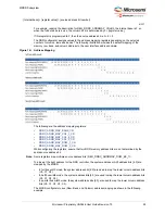
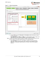
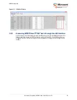
Figure 14 •
Selecting I/O Standard as LVCMOS18 or LPDDRI
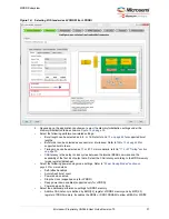
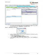
5.
Depending on the application requirement, select the Memory Initialization settings under the
Memory Initialization tab as shown in
.
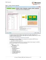
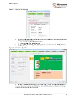
•
Select the following performance-related settings:
•
Burst length can be selected as 4, 8, or 16. Refer to
for supported burst
lengths.
•
Burst order can be selected as sequential or interleaved. Refer to
for
supported burst orders.
•
Timing mode can be selected as 1T or 2T. For more details, refer to
.
•
CAS latency is the delay in clock cycles between the internal READ command and the
availability of the first bit of output data. Select the CAS latency according to the DDR memory
(mode register) datasheet.
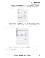
•
Select the following power saving mode settings. Refer to
"Power Saving Modes" section on
for more details.
•
Self-refresh enabled
•
Auto refresh burst count
•
Power down enabled
•
Stop the clock (supported only for LPDDR)
•
Deep power down enabled (supported only for LPDDR)
•
Power down entry time
•
Select the additional performance settings for DDR3 memory.
•
Additive CAS Latency is defined by EMR[5:3] register of DDR2 memory and by MR1[4:3]
register of DDR3 memory. It enables the DDR2 or DDR3 SDRAM to allow a READ or WRITE


