dsPIC33CK Low-Voltage Motor Control Board User’s Guide
DS50002927A-page 32
2020 Microchip Technology Inc.
3.2.2
Power Supply
The Motor Control Board can be powered through coaxial plug J1 or terminal connector
J2. Connector J1 can carry current up to 2.5A and connector J2 can handle up to 24A.
The board is designed to operate in the DC voltage range of 12-48V. DC link capacitors
are placed in parallel with the input to minimize the effects of voltage variation, depend-
ing on the load, and to reduce ripple currents generated by the motor control inverter
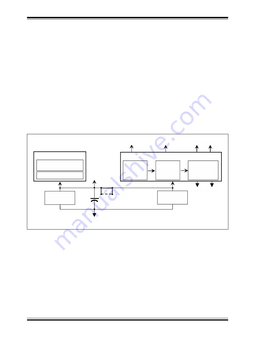
during switching. The power supply block diagram is shown in
The input DC supply connects to the motor control inverter and auxiliary power supply.
The auxiliary power supply section consists of two DC-DC converters and an LDO volt-
age regulator. The MIC28511 synchronous buck converter gen12V output,
which powers the three half-bridge gate drivers used for driving the MOSFETs of the
three-phase inverter. The MCP16301 buck converter generates a +5V output, which is
provided to power the speed/position sensors interfaced via connectors, J7 and J8, and
the Click Boards™ interfaced via the mikroBUS™ sockets, J11 and J12. The fixed 3.3V
LDO MCP1826 gen3.3V, which powers all logical circuits, including the
dsPIC33CK256MP508, operational amplifiers, mikroBUS sockets, USB to UART
converter, user interface elements, temperature sensors, speed/position sensors and
programmer/debugger Interfaces.
FIGURE 3-2:
POWER SUPPLY BLOCK DIAGRAM
The 3.3V digital and analog supply, and ground connections are logically separated
using jumper resistors. In the Motor Control Board design documents, the digital
supply, digital ground, analog supply and analog ground are labeled as +3.3V, DGND,
+3.3 VA and AGND, respectively.
When required, the power to the inverter can be separated by cutting the trace between
net tie NT1. Then, the rest of the circuitry can be powered through the coaxial plug J1
and only the three-phase inverter powered through connector J2. The connection
between the net tie can be bridged back by populating jumper J16, restoring
connections between J1 and J2.
For additional details, refer to
Supply Connectors (J1, J2, J16)”
.
Auxiliary Power Supply
+12V Output
DC-DC
Converter
(MIC28511)
+5V Output
DC-DC
Converter
(MCP16301)
+3.3V Output
LDO
(MCP1826)
+12V
+5V
+3.3 VA
J2
Input Terminal
Connector
J1
Input Jack
Connector
Three-Phase Inverter
MIC4605
x 3
Half-Bridge MOSFET Drivers
Three-Phase Inverter Bridge
+3.3V
VDC
PGND
J16
Jumper
NT1
Net Tie
AGND
DGND


