background image

B1-2

DISASSEMBLY INSTRUCTIONS

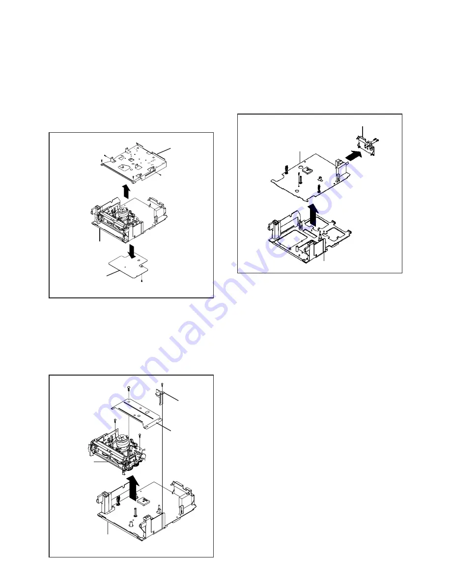
1-7: JACK PLATE AND SYSCON PCB (Refer to Fig. 1-7)

1.
2.
3.
4.
5.

Remove the screw 

1

.

Remove the Syscon PCB in the direction of arrow (A).
Remove the 2 screws 

2

.

Unlock the 2 supports 

3

.

Remove the Jack Plate in the direction of arrow (B).

1-6: DECK CHASSIS (Refer to Fig. 1-6)

1.
2.
3.
4.

5.

Remove the screw 

1

.

Remove the Plate Cover Light.
Remove the 3 screws 

2

.

Disconnect the following connectors:
(CP605, CP1001, CP4001, CP4002 and CP4003).
Remove the Deck Chassis and Shield Cover Deck in
the direction of arrow.

Fig. 1-6

1.
2.
3.
4.
5.
6.

Remove the 2 screws 

1

.

Remove the screw 

2

.

Remove the screw 

3

.

Remove the Deck Shield Plate in the direction of arrow (A).
Remove the screw 

4

.

Remove the Bottom Shield in the direction of arrow (B).

Fig. 1-5

1

Deck Shield Plate

VCR Block

2

1

(A)

(B)

4

3

Plate Cover Light

Syscon PCB

1

2

2

Deck Chassis

2

Fig. 1-7

Jack Plate

1

Deck Holder

Syscon PCB

(A)

3

3

(B)

1-5: DECK SHIELD PLATE AND BOTTOM SHIELD
(Refer to Fig. 1-5)

Bottom Shield

2

2

Shield Cover Deck

Summary of Contents for MVT2139 A Series

Page 1: ...SERVICE MANUAL Design and specifications are subject to change without notice MVT2139 Series A COLOR TELEVISION VIDEO CASSETTE RECORDER ORIGINAL MFR S VERSION A...

Page 2: ...ther there are the portions which are deteriorated around the serviced places serviced or not Check the insulation between the antenna terminal or external metal and the AC cord plug blades And be sur...

Page 3: ...CON IN OUT PRINTED CIRCUIT BOARDS OPERATION MAIN CRT SYSCON SCHEMATIC DIAGRAMS Y C AUDIO CCD HEAD AMP MICON POWER IN OUT CHROMA IF SOUND AMP HI FI IF TV POWER DEFLECTION CRT OPERATION INTERCONNECTION...

Page 4: ...put Impedance VHF UHF 75 ohm CH Coverage 2 69 4A A 5 A 1 A I J W W 1 W 84 Intermediate Picture FP 45 75MHz Frequency Sound FS 41 25MHz FP FS 4 5MHz Preset CH No Stereo Dual TV Sound No Tuner Sound Mut...

Page 5: ...ontrol Volume Yes Level Bright Contrast Sharpness Color Yes Tint Yes Bass Treble Balance No Manual Tracking Yes Play Stop FF Rew Rec OTR T Rec Pause Eject Tape In Symbol Mark Yes Auto Tracking Manual...

Page 6: ...Yes VIDEO PLUS SHOWVIEW G CODE No Auto Clock Yes Forward Reverse Picture Search Yes Reverse Slow No One Touch Playback No Auto CH Memory Yes Closed Caption Yes TV Auto Shut off Function Yes End Call...

Page 7: ...No Terminals Front Video Input RCAx1 Audio Input RCAx1 Other Terminal Head Phone Stereo Mono 3 5mm Rear Video Input RCAx1 Audio Input RCAx1 Video Output RCAx1 Audio Output RCAx1 Euro Scart No Diversit...

Page 8: ...rd hook 3 Remove the Back Cabinet in the direction of arrow Fig 1 1 Front Cabinet 1 2 CRT PCB Refer to Fig 1 2 1 2 3 1 3 TV VCR BLOCK Refer to Fig 1 3 1 2 3 4 1 4 MAIN PCB Refer to Fig 1 4 1 2 3 4 5 6...

Page 9: ...llowing connectors CP605 CP1001 CP4001 CP4002 and CP4003 Remove the Deck Chassis and Shield Cover Deck in the direction of arrow Fig 1 6 1 2 3 4 5 6 Remove the 2 screws 1 Remove the screw 2 Remove the...

Page 10: ...ker R 1 2 3 Link Ass y NOTE 1 2 In case of the Locker R installation check if the two positions of Fig 2 3 B are correctly locked When you install the Cassette Side R be sure to move the Locker R afte...

Page 11: ...orm NOTE 1 2 In case of the Worm installation check if the value of the Fig 2 6 B is correct In case of the Loading Motor installation hook the wire on the Cassette Opener as shown Fig 2 6 C Fig 2 6 B...

Page 12: ...oves Refer to Fig 2 9 A Do not adhere the stains on it When you install the reel clean the shaft and grease it FG 84M If you do not grease noise may be heard in FF REW mode After installing the reel a...

Page 13: ...te Opener Remove the Pinch Roller Block and P5 Arm Ass y 1 2 NOTE Do not touch the Pinch Roller Use gloves In case of the Pinch Roller Block and the Pinch Roller Cam installation install correctly as...

Page 14: ...ion Lever Loading Arm S Unit and Loading Arm T Unit 1 Main Rod Main Loading Gear Tension Lever Loading Arm T Unit Loading Arm S Unit Fig 2 16 A 2 14 CAPSTAN DD UNIT Refer to Fig 2 14 A Remove the Caps...

Page 15: ...Fig 2 18 B Fig 2 18 C Cassette Guide Post Cassette Guide Post 2 17 Remove the Polyslider Washer 1 Remove the Clutch Ass y and Ring Spring Remove the Clutch Lever Remove the Coupling Gear Coupling Spr...

Page 16: ...p up the sides of the Rubber Cap in the direction of the arrow and remove one side of the support Refer to Fig 3 2 2 DISASSEMBLY INSTRUCTIONS GND on the CRT Screwdriver Alligator Clip Support CRT GND...

Page 17: ...sing a blower type IC desoldering machine Refer to Fig 4 2 2 Fig 4 2 NOTE Do not add the rotating and the back and forth directions force on the IC until IC can move back and forth easily after desold...

Page 18: ...8 Thin tip Soldering Iron NOTE When the IC leads are bent during soldering and or repairing do not repair the bending of leads If the bending of leads are repaired the pattern may be damaged So be al...

Page 19: ...op Frequency Generator Front Loading Switch Frequency Modulation Frequency Sub Carrier Forward Generator Ground High Pass Filter I K L M N O P R S H SW Hz IC IF IND INV KIL L LED LIMIT AMP LM LDM LP L...

Page 20: ...or Separation Transistor Tracking Trick Playback Test Point Unregulated Volt Voltage Controlled Oscillator Video Intermediate Frequency Vertical Pulse Voltage Display Video Playback Variable Resistor...

Page 21: ...during PLAY VOL MIN 5 POWER ON total hours and PLAY REC total hours are displayed on the screen Refer to the PREVENTIVE CHECKS AND SERVICE INTERVALS CONFIRMATION OF HOURS USED Can be checked of the I...

Page 22: ...tal hours 16 x 16 x 16 x thousands digit value 16 x 16 x hundreds digit value 16 x tens digit value ones digit value The following standard table depends on environmental conditions and usage Parts re...

Page 23: ...elow 2 TAPE RUNNING SYSTEM When cleaning the tape transport system use the gauze moistened with isopropyl alcohol 3 CYLINDER Wrap a piece of chamois around your finger Dip it in isopropyl alcohol Hold...

Page 24: ...the FF or REW button on the remote step through the ADDRESS until required ADDRESS to be changed is reached Press ENTER to select DATA When DATA is selected it will blink Again step through the DATA u...

Page 25: ...VHS Alignment Tape For 2 heads model VHS Alignment Tape For 2 heads model VHS Alignment Tape For 4 heads model VHS Alignment Tape For 4 heads model VHS Alignment Tape For 4 heads model VHS Alignment T...

Page 26: ...2Y Remove the Operation PCB from the set then connect it with the Syscon PCB If necessary connect CD351 Front A V Jack Input Terminal Short circuit between TP1001 and Ground with the cable JG154 The B...

Page 27: ...tes 20 2gf in the beginning of playback 1 2 USING A CASSETTE TYPE TORQUE TAPE JG100A 1 2 3 After confirmation and adjustment of Tension Post position Refer to item 1 2 load the cassette type torque ta...

Page 28: ...2 as shown in Fig 2 1 B even if you press the Tracking Button to move the envelope The envelope waveform will begin to decrease when you press the Tracking Button Adjust the PG shifter during playback...

Page 29: ...to TP4001 CH 2 to TP1002 and CH 3 to HOT side of Audio Out Jack Playback the VHS Alignment Tape JG001S or JG001T Refer to SERVICING FIXTURE AND TOOLS Press and hold the Tracking Auto button on the rem...

Page 30: ...STMENT PARTS LOCATION GUIDE 5 6 7 8 9 10 1 2 3 4 1 Tension Connect 2 Tension Arm 3 Guide Roller 4 Audio Control Head 5 X value adjustment driver hole 6 7 8 9 10 P4 Post T Brake Spring T Reel S Reel Ad...

Page 31: ...t after unfastening or changing a wire be sure to put the wire back in its original position When you exchange IC and Transistor for a heat sink apply the silicon grease YG6260M on the contract sectio...

Page 32: ...mote control until the SHIFT quantity of the OVER SCAN on right and left becomes minimum 2 10 VERTICAL SHIFT 1 2 3 4 5 Receive the center cross signal from the Pattern Generator Using the remote contr...

Page 33: ...ne Refer to Fig 2 2 Receive the color bar pattern Audio Video Input Press the INPUT SELECT button on the remote control to set to the AV mode Then perform the above adjustments 2 5 A White 100 White 0...

Page 34: ...AL ADJUSTMENTS 2 20 COLOR LEVEL 1 2 3 Receive the color bar pattern RF Input Connect the oscilloscope to TP4201 When setting to the Y LEVEL 100 check if the MAGENTA is 45 10 Refer to Fig 2 6 Fig 2 6 1...

Page 35: ...ng adjustments in section 3 1 1 2 3 4 5 Receive the green raster pattern from the color bar generator Adjust the pair of purity magnets to center the color on the screen Adjust the pair of purity magn...

Page 36: ...TP1001 TP1002 TP4001 CP601_1 C P 8 0 5 B CP820B CD351_1 CD352 OPERATION PCB SYSCON PCB CP2201_2 CD757 A C HEAD CD4001 CP4002 DEW SENSOR CP401 CP403 AC IN FH504 FH503 F502 VR501 VR502 CP502 T501 CP820...

Page 37: ...RY503 RELAY Q511 DC POWER SW PROTECTOR AC DC SW Q514 FEED BACK IC506 LTV 817M VB FEED BACK SW Q507 RECTIFIER D503 D504 D535 D536 2 4 3 1 1 6 4 SW REG DRIVE Q509 Q512 Q505 11 3V REG OPE AMP IC IC504 N...

Page 38: ...EO SD_SYNC TU_VIDEO REAR_A Y C_AUDIO 6 2 3 1 5 Q4005 BIAS CTL 11 4 P CON 5V 1 C ROT RF SW IN AUDIO MUTE HA SW ENV DET Q4006 BIAS OSC Q4003 SW Q4001 Q4002 AUDIO PB SW Q4012 BUFFER COIL BIAS OSC R HA GN...

Page 39: ...ICON IN OUT BLOCK DIAGRAM SDA SCL OSD_R CTL SD_VIDEO CTL V REC_ST_H VD OSD_G AFT_M OSD_B OSD_BLK HD Y C AUDIO CCD HEAD AMP TV CAPSTAN DD UNIT FF REW L 97 73 CTL AMP OUT Q1004 FF REW_SW J701 FRONT_A VC...

Page 40: ...799 SW798 SW796 SW797 SW751 R351_1 R350 W811 C751 C752 R766 R754_1 R761_2 R793_1 W802 R778_1 R772_1 W002 W004 W005 C781 R777_1 R775_1 C779 J701_1 R773_1 R774_1 R771_1 W003 CD352 W006 W001 C382_1 C755_...

Page 41: ...02 C541 R515 R507 R522 C512 C506 R539 R401 Q408 C410 R412 R533 R532 W037 R509 R508 C542 R529 W008 C504 C537 R422 C555 R503 R505 W830 W831 D512 C540 W832 D405 W042 Q507 R519 R 5 4 7 R528 Q510 D536 D503...

Page 42: ...001 TP1002 W078 W080 W075 W081 R685 W100 W076 W178 W255 W186 W273 W275 W220 W193 W192 W195 W219 W218 W182 W184 R4007 W088 W217 W215 W163 HS353 W049 W052 W053 W055 R353 R359 W154 W328 W289 W110 W118 W1...

Page 43: ...4036 R4024 R4023 C4075 C4020 R4052 C4005 C4006 R4010 C4028 R4017 R4022 C4032 C4033 R4021 R4018 R4019 C4029 R4020 R4014 C4022 R4005 C4014 R4047 R4046 R4035 C622 C626 C634 R614 C621 C618_1 C636 C625 R60...

Page 44: ...3V KA C4023 22 6 3V KA C4027 33 6 3V KA C4025 470 6 3V YK C4004 220 6 3V YK C4034 4 7 25V KA C4009 47 6 3V KA X4001 100CT3R502 Q4009 2SA1037AK BUFFER Q4010 2SA1037AK BUFFER Q4005 KTA1266 BIAS CTL Q400...

Page 45: ...2SA1037AK BUFFER AT 5V BACKUP SDA SCL OSD_R OSD_G OSD_B CAP_CTL REEL_T Y C_CS CYL_CTL Y C_CLK OSD_BLK SD_SYNC AT 5V UCON Y C_DATA V REC_ST_H CENTER_LED POWER_FAIL DC GND P CON 5V AT 12V MOTOR_GND CAP...

Page 46: ...140 EIC W878 W880 W996 C688_1 10 16V KA C685 22 16V KA C684 22 16V KA R690 1K 1 2W R613 10K R669 1K 1 4W R668 470 1 4W R689 560 1 2W R686 100 R667 15 1 4W R663 100 R682 100 C608 1 F C694 470 6 3V YK Q...

Page 47: ...20 1 4W R2212 4 7K R2211 4 7K 1 4W C4204 470P CH C4202 27P CH C4216 1 F C4210 470P CH C4213 470P CH C4201 0 01 B C4221 0 001 B C4205 0 01 B C4218 47P CH C4211 470 16V YK C4245 4 7 50V YK C4220 100 16V...

Page 48: ...C634 0 01 B C613 0 1 B C698 0 033 B C614 0 01 B C631 1 F C623 0 0033 B C601 10P CH C615 220P CH C639 0 01 B C644 0 033 B C602 0 01 B C653 0 01 B C661 1 B C640 0 1 B C660 0 1 B C664 1 63V MKT C669 0 0...

Page 49: ...AN POINT DE VUE SECURITE ETANT LES PIECES REPAREES PAR UN ATTENTION HS353 763WSA0021 S107X AUDIO SIGNAL REC OF PRINTING AND SUBJECT TO CHANGE WITHOUT NOTICE NOTE THIS SCHEMATIC DIAGRAM IS THE LATEST...

Page 50: ...1 3 4 5 6 7 8 OF PRINTING AND SUBJECT TO CHANGE WITHOUT NOTICE NOTE THIS SCHEMATIC DIAGRAM IS THE LATEST AT THE TIME W959 C5555 0 0022 B C6309 0 1 B P CON 5V P CON 5V GND P CON 5V G 14 G 13 VMA245 PCB...

Page 51: ...EO SIGNAL OF PRINTING AND SUBJECT TO CHANGE WITHOUT NOTICE NOTE THIS SCHEMATIC DIAGRAM IS THE LATEST AT THE TIME W982 MONITOR_V VIDEO_OUT VIDEO_OUT VIDEO_OUT MONITOR_V TO IN OUT TO Y C AUDIO CCD HEAD...

Page 52: ...SS133 D539 11E1 EIC D540 11E1 EIC D548 1SS133 D537_1 SB290S W845 W803 W830 W831 W832 W822 W823 W848 W824 C527_1 2 2 50V YK C504 22 50V MHE C535 2200 16V MHE C539 3 3 160V MHE C537 1000 25V MHE C538_1...

Page 53: ...EST AT THE TIME CAUTION DIGITAL TRANSISTOR Q407 KRA102MAT SWITCHING Q401 KRA102MAT DEGAUSE SW D413 RMPG06J D402 RMPG06J D401 11E1 EIC D404 1SS133 D405 1SS133 W810 W812 W872 W875 W818 W815 W852 W853 W8...

Page 54: ...L801 100uH B SIGNAL R SIGNAL G SIGNAL OF PRINTING AND SUBJECT TO CHANGE WITHOUT NOTICE NOTE THIS SCHEMATIC DIAGRAM IS THE LATEST AT THE TIME CP803B 52147 0610 1 2 3 4 5 6 CP801_1 A2361WV2 2P 1 2 W836...

Page 55: ...ORMAL NOTE DESCRIBED IN PARTS LIST ONLY CRITICAL FOR SAFETY USE ONES ARE SINCE THESE PARTS MARKED BY CAUTION DANS LA NOMENCLATURE DES PIECES N UTILISER QUE CELLS DECRITES DANGEREUSES AN POINT DE VUE S...

Page 56: ...CH2 UN4001 CYLINDER UNIT ASS Y POWER_FAIL DC X RAY_STOP AT 30V AT 13V UNREG 8V UNREG 8V MOTOR_GND AT 12V AT 5 6V GND GND POWER_FAIL DC CP4202_1 CD351_1 POWER_ON_L CD757 TCA386 J801 CRT SOCKET 9 8 7 6...

Page 57: ...CCD HEAD AMP MICON 10 PB 1 0V 10ms div 9 POWER ON 1 0V 20 s div 2 POWER ON 100mV 0 1 s div 1 PB 0 5V 20 s div 8 POWER ON 0 5V 10ms div 5 REC 10 0V 5us div 3 PB 10mV 20us div 4 PB 0 5V 1ms div DEFLECTI...

Page 58: ...llowing waveforms were measured at the point of the corresponding balloon number in the schematic diagram NOTE H 2 WAVEFORMS 22 50 0V 20 s div 21 50 0V 20 s div 16 200mV 20 s div CHROMA IF 15 100mV 20...

Page 59: ...CRT PCB 203 203 L508 203 203 V801 115 J801 127 215 215 215 123 202 202 215 PCB030 OPERATION PCB 113 117 118 116 206 202 120 121 101 B 202 SP351 119 122 206 133 132 135 202 210 207 107 212 212 PCB070...

Page 60: ...MECHANICAL EXPLODED VIEW 106 102 128 111 204 205 205 205 213 126 125 205 205 214 A 213 129 107 213 110 205 107 108 130 103 104 105 112 112 207 208 201 201 B PCB010 SYSCON PCB TU601 209 109 206 131 124...

Page 61: ...4 302 301 313 307 300 317 309 336 346 321 319 320 AB 316 318 325 347 AB AB AB AA AA AA AA AA AB AB AB AB AB AB 502 501 AD AC AC Applying positions AA AB AC and AD for the grease are displayed for this...

Page 62: ...510 337 340 509 308 344 327 343 326 328 AA AA AB AB AB AA AA AD AA AA AA AA AA AA Applying positions AA AB AC and AD for the grease are displayed for this section Check if the correct grease is applie...

Page 63: ...761WPA0240 HOLDER TV PCB 130 753WUAA006 SPRING EARTH HEAD AMP 131 752WSA0263 SHIELD COVER DECK 132 722000A023 SHEET HWC 133 7220001119 SHEET CSA WARNING 134 723000A927 FILM DECORATION 135 726000A023 S...

Page 64: ...TE HDP 05 26 314 85OA400233 TENSION ARM ASS Y WT H5001 1523D91034 HEAD AUDIO CONTROL HVMXA1072A 315 85OA400231 INCLINED BASE S UNIT H5002 1543D02013 HEAD FULL ERASE HVFHP0032A 316 85OP800358 SPRING LO...

Page 65: ...1SS133T 77 C425 C03L0R713K CC 0 001 UF 2KV R D550 D97U06R81B DIODE ZENER MTZJ6 8B T 77 C426 C0PLRR713K CC 0 001 UF 2KV RR D551 D97U02R21B DIODE ZENER MTZJ2 2B T 77 C430 C0PLRR713K CC 0 001 UF 2KV RR...

Page 66: ...FIXED EVNCYAA03BE3 Q806 TCA0042170 TRANSISTOR SILICON KTC4217 O Y VR502 V1163Q3BTC VOLUME SEMI FIXED EVNCYAA03BQ3 Q1002 0000M00390 PHOTO TRANSISTOR ST 304L P C BOARD ASSEMBLIES Q1003 0002700680 PHOTO...

Page 67: ...2 124120301A EYE LET XRY20X30BD F501 081PC05004 FUSE 51MS050LCC F502 081PC2R504 FUSE 51MS025LCC FB401 043214034F TRANSFORMER FLYBACK 3214034F FH501 06710T0006 HOLDER FUSE EYF 52BC FH502 06710T0006 HOL...

Page 68: ...M5A3 A0I K215046 SPEC NO O R NO...

Reviews: