Measurement Computing USB-1616HS-2 User Manual Download Page 23

USB-1616HS-2 User's Guide 

Functional Details 

23  

Although averaging can be effective, it suffers from several drawbacks:  


Noise in measurements only decreases as the square root of the number of measurements—reducing RMS 
noise significantly may require many samples. Thus, averaging is suited to low-speed applications that can 
provide many samples. 


Only random noise is reduced or eliminated by averaging. Averaging does not reduce or eliminate periodic 
signals. 

Analog output 

The USB-1616HS-2 has two 16-bit, 1 MHz analog output channels. Analog outputs can be updated at a 
maximum rate of 1 MHz. 

The channels have an output range of -10 V to +10 V. Each D/A can continuously output a waveform. In 
addition, a program can asynchronously output a value to any of the D/A channels for non-waveform 
applications, assuming that the D/A is not already being used in the waveform output mode.  

When used to generate waveforms, you can clock the D/As in several different modes. 


Internal output scan clock

: The onboard programmable clock can generate updates ranging from 1 Hz to 

1 MHz. 


External output scan clock

: A user-supplied external output scan clock at the DPR screw terminal. 


External input scan clock

: A user-supplied external input scan clock at APR can pace both the D/A and 

the analog input. 


Internal input scan clock

: The internal ADC scan clock. 

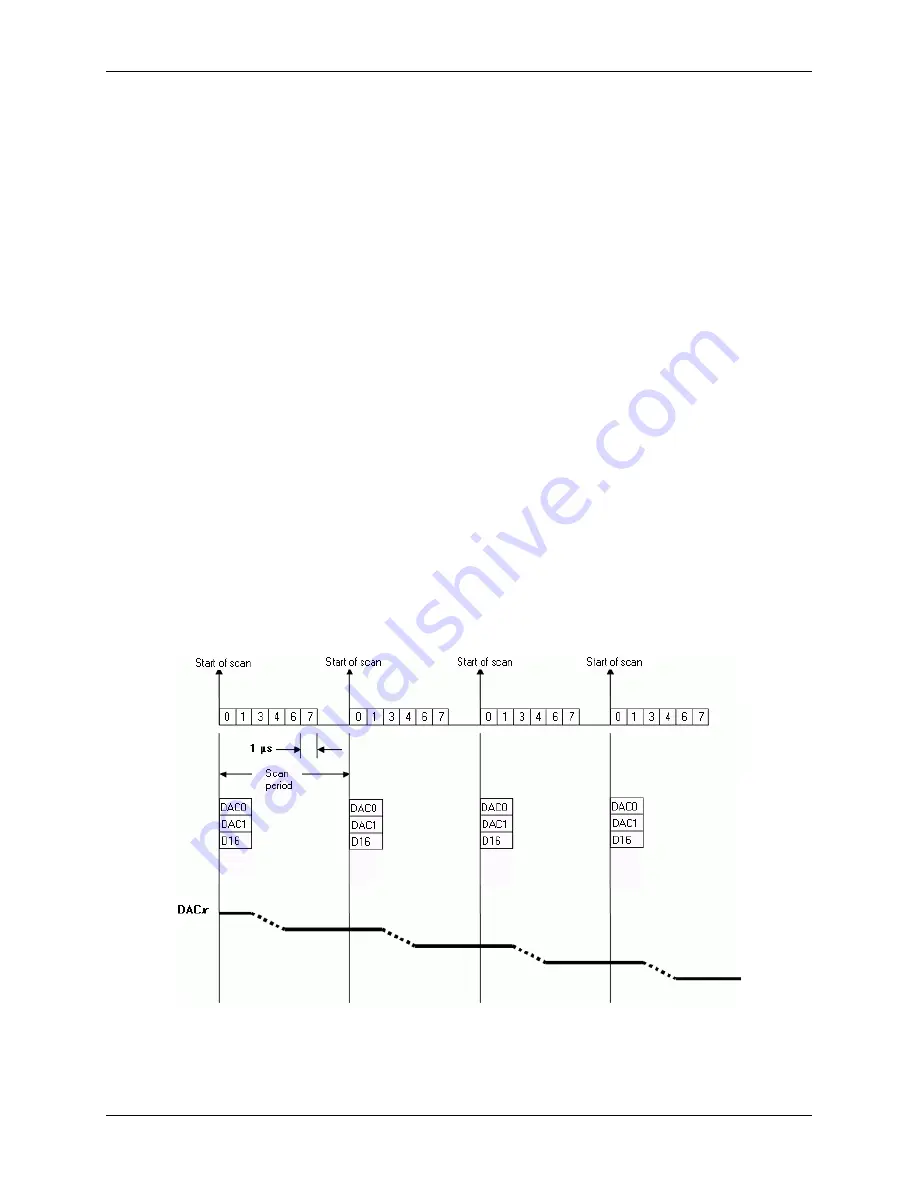
Example: Analog channel scanning of voltage inputs and streaming analog 
outputs 

The example shown in Figure 11 adds two DACs and a 16-bit digital pattern output to the example presented in 
Figure 7 on page 19. 


Figure 11. Analog channel scan of voltage inputs and streaming analog outputs example 

This example updates all DACs and the 16-bits of digital I/O. These updates happen at the same time as the 
output scan clock. All DACs and the 16-bits of pattern digital output are updated at the beginning of each scan.  

Summary of Contents for USB-1616HS-2

Page 1: ......

Page 2: ...USB 1616HS 2 User s Guide Document Revision 2 March 2009 Copyright 2009 Measurement Computing Corporation...

Page 3: ...ion For specific information please refer to the terms and conditions of sale Harsh Environment Program Any Measurement Computing product that is damaged due to misuse or any reason may be eligible fo...

Page 4: ...No license is granted by implication or otherwise under any patent or copyrights of Measurement Computing Corporation All rights reserved No part of this publication may be reproduced stored in a retr...

Page 5: ...rminal pin outs 13 DSUB25F expansion connector 14 Cabling 15 Chapter 3 Functional Details 16 USB 1616HS 2 components 16 USB 1616HS 2 block diagram 18 Synchronous I O mixing analog digital and counter...

Page 6: ...amples of control outputs 38 Detection setpoint details 42 FIRSTPORTC DAC or timer update latency 42 Chapter 4 Calibrating the USB 1616HS 2 44 Chapter 5 Specifications 45 Analog input 45 Accuracy 45 T...

Page 7: ...for the names of manuals and help topic titles and to emphasize a word or phrase For example The InstaCal installation procedure is explained in the Quick Start Guide Never touch the exposed pins or...

Page 8: ...he board has 24 high speed lines of digital I O two timer outputs and four 32 bit counters It provides up to 4 MHz scanning on all digital input lines1 Six banks of removable screw terminal blocks pro...

Page 9: ...erify that the following components are included Hardware USB 1616HS 2 USB cable 2 meter length TR 2U power supply and CA 1 line cord AC to DC power supply cord plugs into the external power connector...

Page 10: ...Software Quick Start pdf This booklet supplies a brief description of the software you received with your USB 1616HS 2 and information regarding installation of that software Please read this booklet...

Page 11: ...tions Figure 1 Single ended voltage connections V1 and V2 and differential thermocouple connections V3 If you are using an AI EXP48 expansion device connect it to the USB 1616HS 2 Make sure you do not...

Page 12: ...rmation on signal connections General information regarding signal connection and configuration is available in the Guide to Signal Connections This document is available on our web site at www mccdaq...

Page 13: ...R Timer 1 T1 Analog In Analog common A Port B Digital common D Dig Ctr I O CH 0 0H FIRSTPORTB Bit 0 B0 CH 8 8L FIRSTPORTB Bit 1 B1 Analog common A FIRSTPORTB Bit 2 B2 CH 1 1H FIRSTPORTB Bit 3 B3 CH 9...

Page 14: ...CH 0 HI 0H FIRSTPORTB Bit 0 B0 CH 0 LO 8L FIRSTPORTB Bit 1 B1 Analog common A FIRSTPORTB Bit 2 B2 CH 1 HI 1H FIRSTPORTB Bit 3 B3 CH 1 LO 9L FIRSTPORTB Bit 4 B4 Analog common A FIRSTPORTB Bit 5 B5 CH 2...

Page 15: ...HS 2 User s Guide Installing the USB 1616HS 2 15 Cabling Use a CA 96A 25 pin expansion cable CA 96A expansion cable to connect to the USB 1616HS 2 s 25 pin expansion connector Figure 3 CA 96A expansio...

Page 16: ...lock diagram information on how to use the signals generated by the board diagrams of signals using default or conventional board settings USB 1616HS 2 components These USB 1616HS 2 components are sho...

Page 17: ...ector Although the USB 1616HS 2 is powered by a USB port on a host PC an external power connector may also be required to provide sufficient power for the USB 1616HS 2 Connect the optional TR 2U power...

Page 18: ...z input clock Sequencer reset DSUB25F Expansion connector External power Connect the optional power supply if the USB cannot supply enough power Figure 6 USB 1616HS 2 functional block diagram Synchron...

Page 19: ...time reduces the maximum acquisition rate You can set the settling time to 1 s 5 s 10 s or 1 ms Example Analog channel scanning of voltage inputs Figure 7 shows a simple acquisition The scan is progr...

Page 20: ...ated CJC channels in the channel array For accurate TC readings associate CJC0 with TC0 CJC1 with TC1 and TC2 CJC2 with TC3 CJC3 with TC4 CJC4 with TC5 and TC6 and CJC5 with TC7 When the AI EXP48 modu...

Page 21: ...stream to the PC via the USB cable Each analog channel requires one microsecond of scan time therefore the scan period can be no shorter than 6 s for this example All of the digital channels are samp...

Page 22: ...ource then the TC junction temperature may be changing and the CJC thermistor will have a larger error Use small diameter instrument grade TC wire Small diameter TC wire has less effect on the TC junc...

Page 23: ...not already being used in the waveform output mode When used to generate waveforms you can clock the D As in several different modes Internal output scan clock The onboard programmable clock can gene...

Page 24: ...uring or after an analog input scan Digital input ports can be part of the scan group and scanned along with analog input channels Two synchronous modes are supported when digital inputs are scanned a...

Page 25: ...signal toward the desired threshold When the input signal is at the threshold some tolerance the sweep will be triggered Before re arming the trigger again move the analog input signal to a level tha...

Page 26: ...re trigger you must use software based triggering to initiate an acquisition No pre trigger post trigger stop event In this simple mode data acquisition starts when the trigger is received and the acq...

Page 27: ...he four counter input signals post debounce A mapped channel can be used to gate the counter decrement the counter latch the current count to the count register Usually all counter outputs are latched...

Page 28: ...od to indicate the start of a scan group latches the count so that the count is updated each time a scan is started Gating on mode Sets the gating option to on for the mapped channel enabling the mapp...

Page 29: ...is equal to T2 and T5 T1 In the example above the input signal goes high at the beginning of time period T1 but never stays high for a period of time equal to the debounce time setting equal to T2 fo...

Page 30: ...ction by going low T5 During time period T5 the input signal again has disturbances that cause the input to not meet the debounce time requirement The output does not change state T6 After time period...

Page 31: ...t pulse but longer than the period of the undesired disturbance as shown in Figure 18 Figure 18 Optimal debounce time for trigger after stable mode Encoder mode Rotary shaft encoders are frequently us...

Page 32: ...at the first trigger is legitimate Figure 19 Representation of rotary shaft quadrature encoder The concentric pattern for B has the same number of window pairs as A except that the entire pattern is r...

Page 33: ...output drive capability and the input impedance of the USB 1616HS 2 Lower values of pull up resistors cause less distortion but also cause the encoder s output driver to pull down with more current Wi...

Page 34: ...annel Example Timer outputs Timer outputs are programmable square waves The period of the square wave can be as short as 1 s or as long as 65535 s Refer to the table below for examples of timer output...

Page 35: ...oint configuration feature you can configure up to 16 detection setpoints associated with channels in a scan group Each setpoint can update the following allowing for real time control based on acquis...

Page 36: ...no action True and False If True then output value 1 If False then output value 2 Window hysteresis mode Above A X A Below A X B Both conditions are checked when in hysteresis mode Hysteresis mode fo...

Page 37: ...value Signal is above 16 bit low limit so 16 bit high limit is not used Less than value Signal is below 16 bit high limit so 16 bit low limit is not used Equal to value Signal is equal to 16 bit high...

Page 38: ...ing a True state shows 1 giving us decimal 2 Setpoint 4 having a True state shows 1 giving us decimal 16 For proper operation the setpoint status register must be the last channel in the scan list Exa...

Page 39: ...is within the shaded region and a different value when the analog input voltage is outside the shaded region 30 h in the example Detection on an analog input timer output updates Update Mode Update o...

Page 40: ...nnel 0 is updated accordingly In this example Channel 3 s analog input voltage is being used to update DAC0 as follows When outside the window low below limit B DAC0 is updated with 3 0 V This update...

Page 41: ...efore the updates for DAC2 only occur when the criteria is met However in the above figure we see that there are two setpoints acting on one DAC We can also see that the two criteria can be met simult...

Page 42: ...han the window Update on True and False uses two update values The update values can drive DACs FIRSTPORTC or timer outputs FIRSTPORTC digital outputs can be updated immediately upon setpoint detectio...

Page 43: ...data that is put into the acquisition stream at the scan rate This data is acquired according to the pre acquisition setup scan group scan period etc and returned to the PC Counters are latched into...

Page 44: ...ion and the other which is available for field calibration You can perform field calibration automatically in seconds with InstaCal and without the use of external hardware or instruments Field calibr...

Page 45: ...I O Maximum usable input voltage common mode voltage CMV Vin Range 10 V 5 V 2 V 1 V 0 5 V 10 5 V maximum Range 0 2 V 0 1 V 2 1 V maximum Signal to noise and distortion 72 dB typical for 10 V range 1...

Page 46: ...ternal power Analog outputs Analog output channels can be updated synchronously relative to scanned inputs and clocked from either an internal onboard clock or an external clock source Analog outputs...

Page 47: ...ut low 0 8 V Output current Output 1 0 mA per pin Sourcing more current may require a TR 2U power supply Digital input pacing Onboard input scan clock external input scan clock APR Digital output paci...

Page 48: ...r an external clock source Table 7 Input sequencer specifications Input scan clock sources two see Note 4 Internal programmable Analog channels from 1 s to 1 s in 20 83 ns steps Digital channels and c...

Page 49: ...input is provided for digital triggering Input signal range 15 V to 15 V maximum Trigger level TTL level sensitive Minimum pulse width 50 ns high 50 ns low Latency One scan period maximum Digital pat...

Page 50: ...type USB 2 0 high speed mode 480 Mbps if available recommended otherwise USB1 1 full speed mode 12 Mbps Device compatibility USB 2 0 recommended or USB 1 1 Environmental Table 13 Environmental specifi...

Page 51: ...nalog In Analog common A Port B Digital common D Dig Ctr I O CH 0 0H FIRSTPORTB Bit 0 B0 CH 8 8L FIRSTPORTB Bit 1 B1 Analog common A FIRSTPORTB Bit 2 B2 CH 1 1H FIRSTPORTB Bit 3 B3 CH 9 9L FIRSTPORTB...

Page 52: ...n A Port B Digital common D Dig Ctr I O CH 0 HI 0H FIRSTPORTB Bit 0 B0 CH 0 LO 8L FIRSTPORTB Bit 1 B1 Analog common A FIRSTPORTB Bit 2 B2 CH 1 HI 1H FIRSTPORTB Bit 3 B3 CH 1 LO 9L FIRSTPORTB Bit 4 B4...

Page 53: ...61326 1 2006 or IEC 61326 1 2005 Shielded wires must be used for all I Os and must be less than 3 meters 9 75 feet in length Clips must be used with the AI EXP48 The host computer must be properly gro...

Page 54: ...Measurement Computing Corporation 10 Commerce Way Suite 1008 Norton Massachusetts 02766 508 946 5100 Fax 508 946 9500 E mail info mccdaq com www mccdaq com...

Reviews: