background image


Chapter 5 

Calibrating the PCI-DAS64/M1/16 

Overview 

The PCI-DAS64/M1/16 provides self-calibration of the analog inputs and outputs, eliminating the need for 
external equipment and user adjustments.


All adjustments are made via 8-bit calibration DACs which are 

referenced to an on-board factory-calibrated standard.


The board is fully calibrated at the factory with 

calibration coefficients stored in nvRAM.


At run time, these calibration factors are loaded into system memory 

and are automatically retrieved each time you specify a different DAC/ADC range. 

You can recalibrate any time using factory voltage standards by selecting the 

Calibrate

 option in 

Insta

Cal. A 

full calibration typically requires less than two minutes. We strongly recommend that you turn your computer 
on, and allow at least 60 minutes for the internal computer case temperature to stabilize prior to calibrating (or 
acquiring data with) the board. 

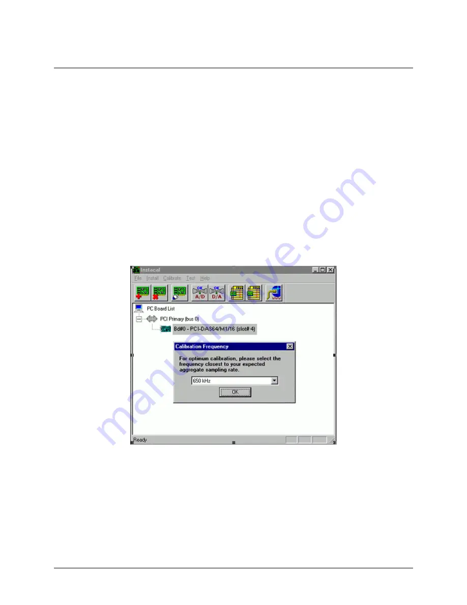
A/D calibration is performed at user-selectable conversion frequencies to reduce any frequency-dependent 
offset effects across the operating range. When you pull down the 

Calibrate

 menu option and click on 

A/D

, a 

dialog opens for you to select a calibration frequency (see 

). We recommend that you select a 

frequency as close as possible to the applications’ sampling frequency. 

Figure 5-1

Figure 5-1. 

Insta

Cal Calibration Frequency dialog 


Table 5-1 lists the available calibration frequencies and recommended sampling frequency ranges. Using this 
table as a guide, a ±1 LSB offset error relative to the calibrated offset is maintained over a given sampling 
frequency range. We recommend that you perform A/D calibration at 100 kHz if you intend to use the entire 
sampling frequency range but do not want to re-calibrate for a given sampling frequency span. In that case, you 
can expect a ±6 LSB offset drift with respect to the calibrated offset over the full 10 Hz to 2 MHz range. 


5-1 

Summary of Contents for PCI-DAS64/M1/16

Page 1: ......

Page 2: ...PCI DAS64 M1 16 Multifunction Analog Digital I O User s Guide Document Revision 1 July 2006 Copyright 2006 Measurement Computing Corporation ...

Page 3: ... that is damaged even due to misuse for only 50 of the current list price I O boards face some tough operating conditions some more severe than the boards are designed to withstand When a board becomes damaged just return the unit with an order for its replacement at only 50 of the current list price We don t need to profit from your misfortune By the way we honor this warranty for any manufacture...

Page 4: ...granted by implication or otherwise under any patent or copyrights of Measurement Computing Corporation All rights reserved No part of this publication may be reproduced stored in a retrieval system or transmitted in any form by any means electronic mechanical by photocopying recording or otherwise without the prior written permission of Measurement Computing Corporation Notice Measurement Computi...

Page 5: ...M1 16 2 2 Configuring the PCI DAS64 M1 16 2 3 Connecting the board for I O operations 2 3 Connectors cables main I O connector 2 3 Pinout main I O connector 2 4 Pin out auxiliary DIO connector 2 7 Field wiring signal termination and conditioning 2 10 Chapter 3 Programming and Developing Applications 3 1 Programming Languages 3 1 Packaged Applications Programs 3 1 Register Level Programming 3 1 Cha...

Page 6: ...nd triggering 6 8 Digital input output 6 8 Interrupts 6 9 Counters 6 9 Pacer 6 10 Power consumption 6 10 Environmental 6 10 Mechanical 6 10 Main connector and pin out 6 10 Differential mode pin out 6 11 Single ended mode pin out 6 12 Digital input output connector and pin out 6 13 v ...

Page 7: ...f manuals and help topic titles and to emphasize a word or phrase For example The InstaCal installation procedure is explained in the Quick Start Guide Never touch the exposed pins or circuit connections on the board Where to find more information The following electronic documents provide relevant information to the operation of your PCI DAS64 M1 16 MCC s Specifications PCI DAS64 M1 16 the PDF ve...

Page 8: ...rbitration among the various functions using the various sections of the SRAM buffer The STC allows simultaneous full speed A D sampling D A updating and gain channel queue sequencing with variable inter sample timing if desired The STC chip performs these functions up to 5 MHz and is available as an OEM component for use in your own designs The board provides bus mastering and scatter gather func...

Page 9: ...ailable in PDF at www mccdaq com PDFmanuals DAQ Software Quick Start pdf This booklet supplies a brief description of the software you received with your PCI DAS64 M1 16 and information regarding installation of that software Please read this booklet completely before installing any software or hardware Optional components If you ordered any of the following products with your board they should be...

Page 10: ...To install your board follow the steps below Install the MCC DAQ software before you install your board The driver needed to run your board is installed with the MCC DAQ software Therefore you need to install the MCC DAQ software before you install your board Refer to the Quick Start Guide for instructions on installing the software 1 2 3 Turn your computer off open it up and insert your board int...

Page 11: ...hat uses Measurement Computing s Universal Library will initialize the hardware according to these selections Connecting the board for I O operations Connectors cables main I O connector Table 2 1 Table 2 1 Main board connector cables accessory equipment lists the board connectors applicable cables and compatible accessory boards Parameter Specification Main connector Shielded SCSI 100 pin D type ...

Page 12: ...9 29 CH19 IN LO CH20 IN HI 78 28 CH20 IN LO CH21 IN HI 77 27 CH21 IN LO CH22 IN HI 76 26 CH22 IN LO CH23 IN HI 75 25 CH23 IN LO CH24 IN HI 74 24 CH24 IN LO CH25 IN HI 73 23 CH25 IN LO CH26 IN HI 72 22 CH26 IN LO CH27 IN HI 71 21 CH27 IN LO CH28 IN HI 70 20 CH28 IN LO CH29 IN HI 69 19 CH29 IN LO CH30 IN HI 68 18 CH30 IN LO CH31 IN HI 67 17 CH31 IN LO D A GND 0 66 16 12V D A OUT 0 65 15 GND D A GND ...

Page 13: ...9 IN CH18 IN 80 30 CH50 IN CH19 IN 79 29 CH51 IN CH20 IN 78 28 CH52 IN CH21 IN 77 27 CH53 IN CH22 IN 76 26 CH54 IN CH23 IN 75 25 CH55 IN CH24 IN 74 24 CH56 IN CH25 IN 73 23 CH57 IN CH26 IN 72 22 CH58 IN CH27 IN 71 21 CH59 IN CH28 IN 70 20 CH60 IN CH29 IN 69 19 CH61 IN CH30 IN 68 18 CH62 IN CH31 IN 67 17 CH63 IN D A GND 0 66 16 12V D A OUT 0 65 15 GND D A GND 1 64 14 12V D A OUT 1 63 13 GND PC 5V 6...

Page 14: ...stamped Pins 1 50 Pins 1 50 are on the long side of the D connector Pins 51 100 are on the short side of the D connector Key Key The red stripe identifies pin 1 The red stripe identifies pin 51 Strain relief is Stamped Pins 51 100 Figure 2 1 C100HD50 x cable 100 50 51 1 100 50 51 1 Figure 2 2 C100MMS x cable 2 6 ...

Page 15: ... DIG GND FIRSTPORTB Bit 7 5 6 FIRSTPORTC Bit 7 FIRSTPORTB Bit 6 7 8 FIRSTPORTC Bit 6 FIRSTPORTB Bit 5 9 10 FIRSTPORTC Bit 5 FIRSTPORTB Bit 4 11 12 FIRSTPORTC Bit 4 FIRSTPORTB Bit 3 13 14 FIRSTPORTC Bit 3 FIRSTPORTB Bit 2 15 16 FIRSTPORTC Bit 2 FIRSTPORTB Bit 1 17 18 FIRSTPORTC Bit 1 FIRSTPORTB Bit 0 19 20 FIRSTPORTC Bit 0 DIG GND 21 22 FIRSTPORTA Bit 7 NC 23 24 FIRSTPORTA Bit 6 DIG GND 25 26 FIRST...

Page 16: ... 7 FIRSTPORTC BIT 6 FIRSTPORTC BIT 5 FIRSTPORTC BIT 4 FIRSTPORTC BIT 3 FIRSTPORTC BIT 2 FIRSTPORTC BIT 1 FIRSTPORTC BIT 0 FIRSTPORTA BIT 7 FIRSTPORTA BIT 6 FIRSTPORTA BIT 4 FIRSTPORTA BIT 3 FIRSTPORTA BIT 2 FIRSTPORTA BIT 1 FIRSTPORTA BIT 0 FIRSTPORTB BIT 2 FIRSTPORTB BIT 3 FIRSTPORTB BIT 4 FIRSTPORTB BIT 5 FIRSTPORTB BIT 6 FIRSTPORTB BIT 7 NC FIRSTPORTB BIT 1 GND NC GND NC GND NC GND GND 5V FIRST...

Page 17: ... 4 25 Port C 4 13 Port B 3 7 Port B 3 14 Port C 3 26 Port C 3 15 Port B 2 8 Port B 2 16 Port C 2 27 Port C 2 17 Port B 1 9 Port B 1 18 Port C 1 28 Port C 1 19 Port B 0 10 Port B 0 20 Port C 0 29 Port C 0 21 GND 11 GND 22 Port A 7 30 Port A 7 23 N C 12 N C 24 Port A 6 31 Port A 6 25 GND 13 GND 26 Port A 5 32 Port A 5 27 N C 14 N C 28 Port A 4 33 Port A 4 29 GND 15 GND 30 Port A 3 34 Port A 3 31 N C...

Page 18: ...ctly or by combining the BP40 37 adapter and C37FF x or C37FFS x cable SCB 37 37 conductor shielded signal connection screw terminal box Details on are available on our web site at www mccdaq com cbicatalog cbiproduct asp dept_id 196 pf_id 1166 CIO MINI37 37 pin universal screw terminal board Details are available on our web site at www mccdaq com cbicatalog cbiproduct asp dept_id 102 pf_id 255 CI...

Page 19: ...e drivers for your board If the package you own does not have drivers for the board please fax or e mail the package name and the revision number from the install disks We will research the package for you and advise how to obtain drivers Some application drivers are included with the Universal Library package but not with the application package If you have purchased an application package direct...

Page 20: ...t A D Internal Pacer Out 24 bits DIO FIRSTPORTA 7 0 FIRSTPORTB 7 0 FIRSTPORTC 7 0 DIN 3 0 DOUT 3 0 PortA PortB PortC Control Inputs Outputs Boot EEPROM PCI Bridge w BUS Master 16 DMA C 0 H DMA CH1 PCI Bus 5V 32 bit 33 M z H Holding REG Queue Buffer 8K DAC 0 1 Buffer 16K ADC Buffer 8K CTR1 GATE CTR1 CLK CTR1 OUT Analog In 64 CH single ended 32 CH differential 16 bit ADC Mux Gain Figure 4 1 PCI DAS6...

Page 21: ...16 board provides two high speed 5V 16 bit analog outputs The outputs are updated via on board 16 K FIFO buffer and provide a 100 kHz max update rate Repetitive D A based waveforms can be stored in on board memory and generated without requiring ongoing PCI bus transfers The outputs provide rated accuracy to 15 mA are short circuit protected 25 mA limit and are cleared to 0 volts on power up or re...

Page 22: ...ure to stabilize prior to calibrating or acquiring data with the board A D calibration is performed at user selectable conversion frequencies to reduce any frequency dependent offset effects across the operating range When you pull down the Calibrate menu option and click on A D a dialog opens for you to select a calibration frequency see We recommend that you select a frequency as close as possib...

Page 23: ...alibration helps assure your board operates at the same temperature at which it was calibrated Calibration theory Offset calibration for the analog front end is performed via adjustments of the ADC itself Front end gain adjustment is performed only via the ADC reference This strategy was chosen since the gain tolerance of the in amp circuit is quite good and there is adequate gain tuning range usi...

Page 24: ...s Offset adjustments for the analog outputs are made in the output buffer section The tuning range of this adjustment yields maximum DAC and output buffer offsets Analog output calibration is shown in This circuit is duplicated for both DAC0 and DAC1 Figure 5 3 Figure 5 3 Analog out calibration Ref DAC Gain Adjust Analog Out Offset Adjust Trim DAC Coarse Trim DAC Fine Trim DAC Coarse Trim DAC Fine...

Page 25: ...ternal analog analog trigger in External digital Programmable active high or active low level or edge A D gating modes External analog Software configurable for Above or below reference Positive or negative hysteresis In or out of window Trigger levels set by DAC0 and or DAC1 A D trigger sources External digital A D start trigger in and A D stop trigger in External analog Analog Trigger In A D tri...

Page 26: ...which correspond to the range value selected in cbAInScan These coefficients remain unchanged throughout the scan Errors of up to 25 counts may be incurred when switching gains while in bipolar or unipolar mode only conditions 4 and 5 Errors of up to 500 counts may be incurred when mixing unipolar bipolar modes conditions 6 and 7 Accuracy A 100 kS s sampling rate single channel operation and a 60 ...

Page 27: ...d can be calculated by summing these component errors Worst case errors are realized only in the unlikely event that each of the component errors are at their maximum level and causing error in the same direction Crosstalk Crosstalk is defined here as the influence of one channel upon another when scanning two channels at the maximum rate A full scale 100 Hz triangle wave is input on channel 1 and...

Page 28: ... peak bin spread divided by 6 6 Analog output Table 9 Analog output specifications Resolution 16 bits Number of channels 2 Voltage range 5 V Monotonicity Guaranteed monotonic over temperature Analog output zero drift 1 6 LSB C Overall analog output drift 4 0 LSB C Slew rate 2 5 V µs Settling time FS step to 0008 6µs max all ranges Current drive 15 mA Output short circuit duration Indefinite 25 mA ...

Page 29: ...Table 13 Digital I O specifications Output 74LS175 Digital type main connector Input 74LS244 Configuration Four inputs four outputs DIN0 through DIN3 DOUT0 to DOUT3 Output high voltage IOH 0 4 mA 2 7 V min Output low voltage IOL 8 mA 0 5 V max Input high voltage 2 0 V min 7 volts absolute max Input low voltage 0 8 V max 0 5 volts absolute min Digital type digital I O connector 82C55 Number of I O ...

Page 30: ...DAC sequence completes DAC_FIFO_1 4_EMPTY Interrupt is generated DAC FIFO is empty DAC_HIGH_CHANNEL Interrupt is generated when the DAC high channel output is updated DAC interrupt sources software programmable DAC_RETRANSMIT Interrupt is generated when the end of a waveform sequence has occurred in retransmit mode External interrupt Interrupt is generated via edge sensitive transition on the Exte...

Page 31: ...lectable as SSH OUT default or D A PACER OUT Internal pacer crystal oscillator 40 MHz Frequency accuracy 50 ppm Power consumption Table 17 Power specifications 5 V 2 9 A typical 3 3 A max 12 V 10 mA max Environmental Table 18 Environmental specifications Operating temperature range 0 to 50 C Storage temperature range 40 to 100 C Humidity 0 to 95 non condensing Mechanical Table 19 Mechanical specif...

Page 32: ...LO 69 CH29 IN HI 20 CH28 IN LO 70 CH28 IN HI 21 CH27 IN LO 71 CH27 IN HI 22 CH26 IN LO 72 CH26 IN HI 23 CH25 IN LO 73 CH25 IN HI 24 CH24 IN LO 74 CH24 IN HI 25 CH23 IN LO 75 CH23 IN HI 26 CH22 IN LO 76 CH22 IN HI 27 CH21 IN LO 77 CH21 IN HI 28 CH20 IN LO 78 CH20 IN HI 29 CH19 IN LO 79 CH19 IN HI 30 CH18 IN LO 80 CH18 IN HI 31 CH17 IN LO 81 CH17 IN HI 32 CH16 IN LO 82 CH16 IN HI 33 LLGND 83 LLGND 3...

Page 33: ... 0 16 12 V 66 D A GND 0 17 CH63 IN 67 CH31 IN 18 CH62 IN 68 CH30 IN 19 CH61 IN 69 CH29 IN 20 CH60 IN 70 CH28 IN 21 CH59 IN 71 CH27 IN 22 CH58 IN 72 CH26 IN 23 CH57 IN 73 CH25 IN 24 CH56 IN 74 CH24 IN 25 CH55 IN 75 CH23 IN 26 CH54 IN 76 CH22 IN 27 CH53 IN 77 CH21 IN 28 CH52 IN 78 CH20 IN 29 CH51 IN 79 CH19 IN 30 CH50 IN 80 CH18 IN 31 CH49 IN 81 CH17 IN 32 CH48 IN 82 CH16 IN 33 LLGND 83 LLGND 34 CH4...

Page 34: ...NC 4 DIG GND 5 FIRSTPORTB Bit 7 6 FIRSTPORTC Bit 7 7 FIRSTPORTB Bit 6 8 FIRSTPORTC Bit 6 9 FIRSTPORTB Bit 5 10 FIRSTPORTC Bit 5 11 FIRSTPORTB Bit 4 12 FIRSTPORTC Bit 4 13 FIRSTPORTB Bit 3 14 FIRSTPORTC Bit 3 15 FIRSTPORTB Bit 2 16 FIRSTPORTC Bit 2 17 FIRSTPORTB Bit 1 18 FIRSTPORTC Bit 1 19 FIRSTPORTB Bit 0 20 FIRSTPORTC Bit 0 21 DIG GND 22 FIRSTPORTA Bit 7 23 NC 24 FIRSTPORTA Bit 6 25 DIG GND 26 F...

Page 35: ...missions Immunity EN55024 EN61000 4 2 1995 Electrostatic Discharge immunity Criteria A EN61000 4 3 1997 Radiated Electromagnetic Field immunity Criteria A EN61000 4 4 1995 Electric Fast Transient Burst immunity Criteria A EN61000 4 5 1995 Surge immunity Criteria A EN61000 4 6 1996 Radio Frequency Common Mode immunity Criteria A EN61000 4 8 1994 Power Frequency Magnetic Field immunity Criteria A EN...

Page 36: ...Measurement Computing Corporation 10 Commerce Way Suite 1008 Norton Massachusetts 02766 508 946 5100 Fax 508 946 9500 E mail info mccdaq com www mccdaq com ...

Reviews: