


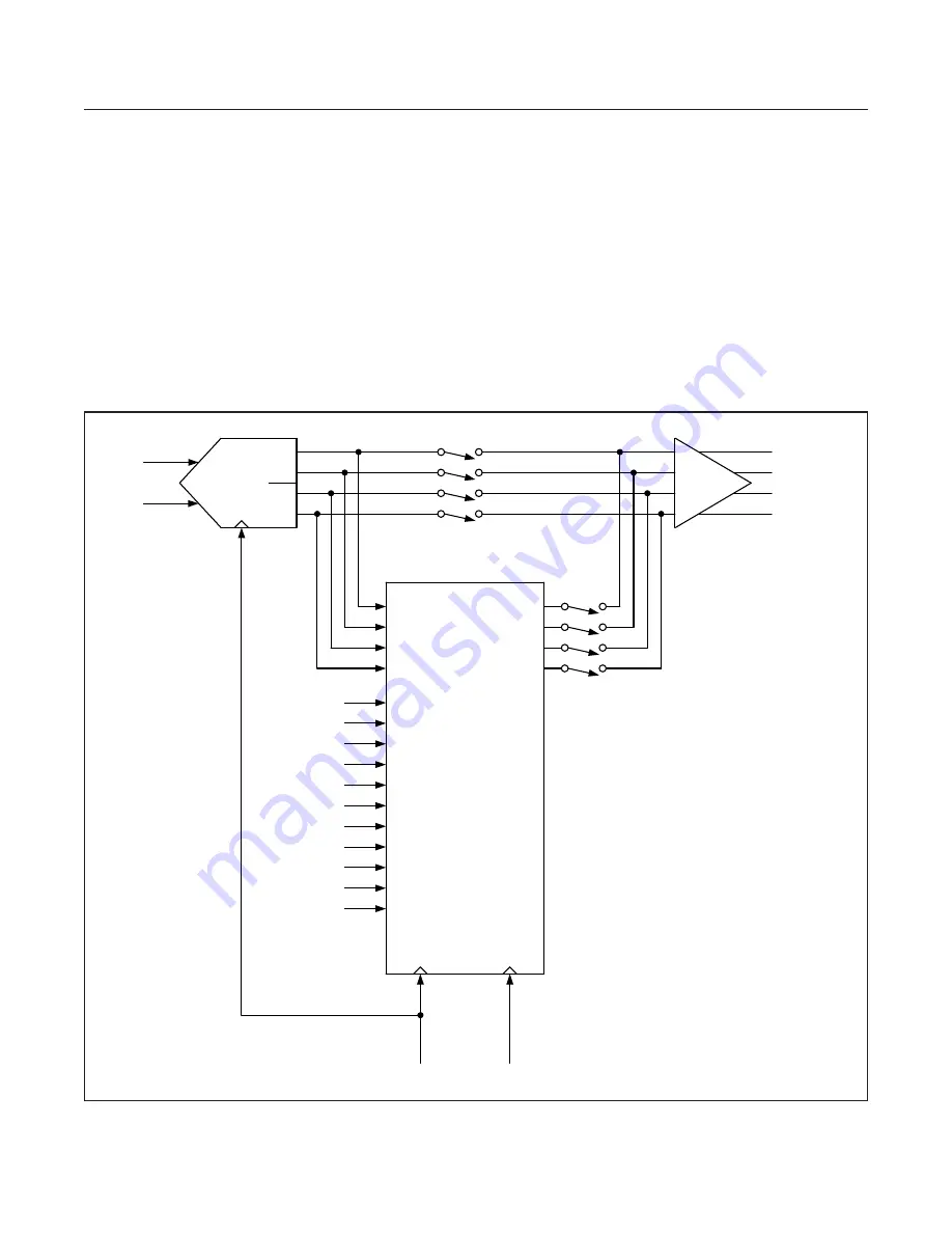
The ADC data is loaded, in parallel, into four holding
registers that correspond to four ADC outputs. Holding
registers are 16 bits long and are clocked by the ADC
clock. At the end of the 16-bit ADC cycle, the data is trans-
ferred into four shift registers and shifted serially to the
output during the next 16-bit ADC cycle. Shift regis ters are
clocked by a serial clock that must be chosen fast enough
so that all data is shifted out before the next set of data
is loaded from the ADC. An all-zero pattern follows the
data after all valid ADC data are streamed to the output. A
DATASYNC signal is used to signal the beginning of each
valid 16-bit data slice. In addition, there is a TIME_SYNC
signal that is output every 128 to 16,384 cycles of the
ADC clock.
Given that the serial clock has to run multiple times
faster than the ADC clock, the use of the DSP interface is
limited to narrowband signals that don’t require a high
ADC sampling clock frequency.
Figure 2. DSP Interface Top Level Connectivity and Control Signals
BIT 0
BIT 1
BIT 2
BIT 3
STRM_EN
STRM_START
STRM_STOP
STRM_COUNT<2:0>
DIEID<1:0>
STRM_BITS<1:0>
FRM_COUNT<27:0>
STAMP_EN
DAT_SYNCEN
TIME_SYNCEN
STRM_RST
CLK_ADC
CLK_SER
CLK_ADC
CLK_SER
CONTROL
SIGNALS
FROM 3-WIRE
INTERFACE
DATA_OUT
CLK_SER
DATA_SYNC
TIME_SYNC
STRM_EN
STRM_EN
ADC
I
PIN 13
PIN 12
PIN 10
PIN 11
OUTPUT
DRIVER
Q
www.maximintegrated.com
Maxim Integrated
│
23
MAX2771
Multiband Universal GNSS Receiver


