background image

28

Chapter 5. Quick Installation Guide

DevKey

- 16 bytes unique AES-128 key

These keys are programmed by MatchX and stored in a special region of the nonvolatile memory

of the Dialog microcontroller. They will be preserved during flashing of the new firmware, however
they will be lost by performing full flash erase. The default values are defined in

lora\param.c

.

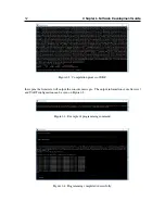
In Dev Kit Firmware the values of these keys are printed on UART console on power up, see Figure
5.4. On default DKF configures pins 5 and 6 on the J102 connector to be UART TX and RX
respectively, a UART-to-USB converter needs to be connected to these pins to see the messages.

Figure 5.4: Displaying the keys on UART console.

The values of DevEUI, AppEUI and DevKey can also be changed from UART console by using

param

command. The syntax is as follow:

param

x value

where x = 0 for DevEUI, 1 for AppEUI and 2 for DevKey, value is a hexadecimal value to be

set.

When value field is not specified the command will output current value of the parameter

(except DevKey, which will not be shown).

DevKey is a AES-128 encryption key used for secure communication. It should be kept secret

and only known to the sensor owner, this is why it is recommended to not display it on the UART
in a final version of the firmware by removing

#define DEBUG

line in

param.c

file. It is also

recommended to change its value before registering the node on the server.

5.6

Region Selection

Dev Kit Firmware implements different regional settings according to regulations applicable to
these regions. By default the board determines which settings to choose by reading the jumpers
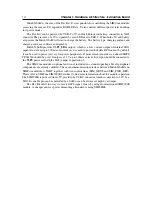
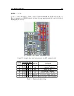
configuration on connector J103 during startup. Jumpers placement is shown on Figure 5.5 and
configuration settings in Table 5.1.

The jumper configuration is read only if the settings are not programmed to internal memory

of the module. It is possible to program these settings using UART similarly to programming the
DevEUI in paragraph 5.5. In this case the jumper values are ignored and J103 pins can be used as
regular GPIOs. The syntax is as follow:

Summary of Contents for LPWAN

Page 1: ...MatchX Dev Kit LoRa Development Board with Grove Sensors User Guide Rev 1 0...

Page 2: ...IO No part of the specifications may be reproduced in any form or by any means or used to make any derivative such as translation transformation or adaptation without permission from MatchX GmbH All...

Page 3: ...n out and pin description of the SoM module 7 2 1 1 Dimensions 9 2 2 Operating frequency bands 10 2 2 1 EU 863 870MHz ISM Band 10 2 2 2 US 902 928MHz ISM Band 10 2 2 3 Australia 915 928MHz ISM Band 10...

Page 4: ...g a node on MarchX server 26 5 5 Setting DevEUI AppEUI and DevKey 27 5 6 Region Selection 28 6 Software Development Guide 30 6 1 References 30 6 2 Prerequisites 30 6 3 Software development under Windo...

Page 5: ...main differences between these two versions are listed in Table 1 1 number Parameter US EU Operating Frequency Band 902 928MHz 863 870MHz Maximum Output Power 17dBm 14dBm Lora BW 500k 125kHz 125kHz S...

Page 6: ...he Core module 1 2 1 Hardware integrated MatchX Core System on Module 18 5dBm output power in 868MHz 915MHz 146dBm sensitivity of LoraWAN packets integrated Semtech SX1276 LoRa and Bluetooth Low Energ...

Page 7: ...pins in Table 2 1 On top of the module there are two UF L RF connectors the one on the left is the LoRa antenna connector a suitable 868MHz in EU and 915MHz in US 50 Ohm antenna is expected to be con...

Page 8: ...battery voltage 2 7V to 4 2V 2 By supplying 5V on the VBUS pin If both power sources are present the battery will be charged form 5V power supply The charging current and charging characteristics for...

Page 9: ...t no voltage higher than V3P3_LDO is presented to any GPIO This may happen when powering external devices that connect to SoM module from a boost converter Figure 2 2 Block diagram of the Core module...

Page 10: ...nally to the 3 mandatory channels 5 additional channels are defined The list of all preconfigured channels can be found in Table 2 4 Spreading Factor Bit rate Range depends Time on air ms 0 1 duty cyc...

Page 11: ...ess 50 29 O 869 400 MHz to 869 650 MHz 25 mW e r p 0 1 duty cycle or polite spectrum access 54a 130 P 869 400 MHz to 869 650 MHz 500 mW e r p 10 duty cycle or polite spectrum access 54b 30 Q 869 700 M...

Page 12: ...30 MHz 7 905 10 MHz 4 904 50 MHz 8 905 30 MHz Table 2 5 Modules operating frequencies uplink in US 902 928MHz ISM Band Channel number Frequency Channel number Frequency 1 915 20 MHz 5 916 00 MHz 2 91...

Page 13: ...Evaluation Board 3 1 Block Diagram The development board comprises of two main subsystems 1 MatchX SoM with LoRa and Bluetooth radios 2 SIMCom SIM7000E NB IOT module with 3G 4G and GPS Figure 3 1 Bloc...

Page 14: ...ault it can be used to power just very low power peripherals If more current is needed a onboard SMPS TPS62740 should be used It outputs a 3 3V up to 300mA current Its output should be connected to th...

Page 15: ...IOT module with 3G 4G and GPS MatchX SoM module with LoRa and Bluetooth SIM28ML GPS receiver 3 3V low power converter for sensors supply PCA6416A I2C I O expander 3 3V LDO for powering the optional SI...

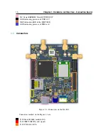
Page 16: ...I OT LED indicating presence of USB 5V NET indication LED of the SIM7000E LED indicating presence of SIM card 3 3 Connectors Figure 3 3 Connectors on the Dev Kit Connectors marked on the Figure 3 3 a...

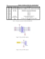
Page 17: ...ctor X401 S2B PH SM4 TB Lithium battery connector USB C connector 5V supply and programming SIM card socket for SIM7000E 3 3 1 Connectors pin out Figure 3 4 Pin out of the Dev Kit The J102 connector s...

Page 18: ...Main I2C bus connected with J104 jumper 4 P4_2 I2C_SDA Main I2C bus connected with J108 jumper 5 P1_4 Not used 6 P1_6 Not used 7 P0_7 Not used 8 P3_3 Not used 9 P3_4 PS_EN controls enable pin of TPS62...

Page 19: ...t and its state can be read and set by the I2C commands Additionally there is a interrupt line EXP_INT that is being driven by the PCA6416A when input IO changes it state Figure 3 7 Pin out of J103 co...

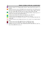
Page 20: ...jumper in position 2 3 selects the V3P3_LDO output from integrated LDO of the SoM module J111 J112 connect the P1_3 and P0_7 to Grove D1 and D2 lines J104 J108 connect the P4_2 and P4_3 to I2C_SDA and...

Page 21: ...by a 0R resistor by default J403 connects power to the input of the low power 3 3V converter the source of the power is USB 5V or battery if the 5V is not present J400 test connector of the VCC_SIM by...

Page 22: ...f the low power 3 3V converter low in the lower position pulls this line up test point connected to the interrupt line of the temperature sensor PTC_OS test point connected to the power good pin of lo...

Page 23: ...the Fan Module and the LED Module that controlled by digital GPIOs D0 and D1 The following table shows the pin out of the Grove digital connector Pin Name Function 1 D0 Primary Digital I 0 2 D1 Second...

Page 24: ...of the Grove UART connector Pin Name Function 1 RX Serial receive 2 TX Serial transmit 3 VCC Power for Grove module 4 GND Ground for Grove module Table 4 3 Pin out of the Grove UART connector 4 4 Grov...

Page 25: ...s or Linux OS 5 2 Connections 5 2 1 Power The Dev Kit is equipped with battery connector As long as the battery is charged there is no other connection required for the Dev Kit to work Charging If the...

Page 26: ...l come with a QR code sticker which gives the Serial Number of the device By typing in the S N at the registration of the MatchX LPWAN Cloud the preprogrammed APP EUI MAC address and DevKey will be as...

Page 27: ...ity in LoRaWAN network and Over the Air Activation OTTA 3 different keys have to be programmed into every end node DevEUI 6 bytes global end device ID in IEEE EUI48 address space that uniquely identif...

Page 28: ...ld is not specified the command will output current value of the parameter except DevKey which will not be shown DevKey is a AES 128 encryption key used for secure communication It should be kept secr...

Page 29: ...settings Figure 5 5 Jumpers placement for region selection EU region selected Region Jumper Position Region Description number 3 2 1 0 00 0 0 0 0 EU Europe region 01 0 0 0 1 AS1 Asia AS923MHz ISM Band...

Page 30: ...e to get familiar with the following documents available on Dialog Semiconductors website DA14680 01 DS Datasheet Dialog Semiconductor UM B 057 SmartSnippets Studio user guide User manual Dialog Semic...

Page 31: ...older for example SmartSnippet workspace folder DKF folder contains a make file which can be executed by navigating to the firmware folder and typing make in the command line window This command will...

Page 32: ...lation process of DKF these pins the firmware will output the console messages The output information sent after reset and UART configuration can be seen on Figure 6 5 Figure 6 3 Example of programmin...

Page 33: ...e It offers makefile project import capabilities In order to import the project open the SmartSnippet IDE The folder structure should be the same as in previous section both SDK and DKF should be in S...

Page 34: ...Workspace like on Figure 6 7 Figure 6 7 Import existing project window Click Next On the next window navigate to the script folder that should be located in sdk_root utilities scripts See Figure 6 8...

Page 35: ...a_initial_flash_jtag_win script by right clicking on it and pressing Duplicate then renaming it The Argument section has to be modified to contain correct path to compiled firmware The variables value...

Page 36: ...d the Dialog s Semiconductor SmartSnippets DA1468x SDK in the example the SDK version 1 0 8 1050 1 has been used and MatchX Dev Kit Frmware Both SDK and Dev Kit Firmware should be put in one folder fo...

Page 37: ...K and software support Over The Air software update Mobile App for Android Free cloud service for managing and visualizing sensors data 7 2 Hardware environment The MatchX Dec Kit is mainly designed f...

Page 38: ...r Lora both the transmission and receive performance are listed in Table 7 2 and Bluetooth can be found in Table 7 3 Item Value TX Max 18 5dBm RX down to 148dBm Table 7 2 Lora RF performance For Bluet...

Page 39: ...of the core module 7 2 3 Antenna characteristics The SoM module is equipped with two U FL connectors 2 4GHz for Bluetooth and one for 868MHz 915MHz in US version LoRa antenna The parameters of the rec...

Page 40: ...40 Chapter 7 Product specification 7 3 Dimensions Figure 7 1 Dimension of the Dev Kit top view all dimensions in mm...

Page 41: ...7 4 Certification 41 7 4 Certification CE and FCC certification pending...

Reviews: