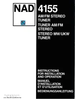
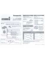
background image

ST-15S1

Please use this service manual with referring to the user guide ( D.F.U. ) without fail.

Service
Manual

ST-15S1 /

N1G/N1S

Part no. 90M22CW855010

First Issue 2006.09

MZ

TABLE OF CONTENTS

SECTION 

PAGE

 1. TECHNICAL SPECIFICATIONS 

........................................................................................... 1

  2.  FACTORY / SERVICE MODE ............................................................................................... 2

  3.  WRITING MAIN MICROPROCESSOR PROCEDURE ........................................................ 3

  4.  UPDATE DAB MICROPROCESSOR PROCEDURE ..........................................................12
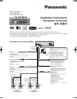
 5. WIRING DIAGRAM 

..............................................................................................................21

  6.  BLOCK DIAGRAM .............................................................................................................. 23

 7. SCHEMATIC DIAGRAM 

..................................................................................................... 25

 8. PARTS LOCATION ............................................................................................................. 29

  9.  MICROPROCESSOR AND IC DATA .................................................................................. 35

 10.  EXPLODED VIEW AND PARTS LIST ................................................................................ 43

 11.  ELECTRICAL PARTS LIST ..................................................................................................47

 12.  ABOUT REPLACE THE MICROPROCESSOR WITH A NEW ONE .................................. 59

DAB / FM / AM Tuner

S

T

-1

5

S

1

DISPLAY

DISPLAY

TUNED

TUNED

STEREO

STEREO

DOWN

DOWN

TUNING/PRESET

TUNING/PRESET

UP

UP

RDS

RDS

SECONDARY

SECONDARY

DAB/FM/AM TUNER ST-15S1

DAB/FM/AM TUNER ST-15S1

BAND

BAND

SELECT

SELECT

AUTO

AUTO
TUNE

TUNE

MENU

MENU

ENTER

ENTER

MEMO

MEMO

POWER ON/OFF

POWER ON/OFF

Summary of Contents for ST-15S1/N1G

Page 1: ...DURE 12 5 WIRING DIAGRAM 21 6 BLOCK DIAGRAM 23 7 SCHEMATIC DIAGRAM 25 8 PARTS LOCATION 29 9 MICROPROCESSOR AND IC DATA 35 10 EXPLODED VIEW AND PARTS LIST 43 11 ELECTRICAL PARTS LIST 47 12 ABOUT REPLAC...

Page 2: ...al Department at above mentioned address 060607MZ USA MARANTZ AMERICA INC 100 CORPORATE DRIVE MAHWAH NEW JERSEY 07430 USA EUROPE TRADING MARANTZ EUROPE B V P O BOX 8744 BUILDING SILVERPOINT BEEMDSTRAA...

Page 3: ...1 kHz Channel separation 100 dB 1 kHz Selectivity 40 dB at adjacent channel Frequency response 0 5 0 5 dB 5 Hz 20 kHz Digital output Optical Coaxial Sampling frequency 48 kHz Aerial terminal 75 F fema...

Page 4: ...sor has been initialized all the button settings are reset to the default values the values set upon shipment from the factory B SERVICE MODE 1 Microprocessor Version check 1 Connect mains cord to the...

Page 5: ...001JIG Writing software flashprog16lx v01l11 exe Writing data Marantz_DABxxxx mhx NOTE xx is a revision number INSTALL PROCEDURE Double click flashprog16lx v01l11 exe 3 WRITING MAIN MICROPROCESSOR PRO...

Page 6: ...4 Click Yes Click Next Yes Next...

Page 7: ...5 Check Complete and click Next Click Install Complete Next Install...

Page 8: ...6 The status bar appears Click Finish Finish...

Page 9: ...ains cord to the unit Press the POWER ON OFF button and turn on the unit Launch up the FUJITSU Flash MCU Programmer FMC16LX Connection Click Start programs FUJITSU FLASH MCU Programmer and FMC16LX Win...

Page 10: ...8 Click Set Environment Choose the using serial port and click OK Set Environment Serial Port OK...

Page 11: ...Choose MB90F352 C S CS in Target Microcontroller Choose 4MHz in Crystal Frequency Click Open Select writing data and click Open Target Microcontroller MB90F352 C S CS Crystal Frequency 4MHz Open Open...

Page 12: ...10 Click Full Operation D E B P Click OK Click OK Full Operation D E B P OK OK...

Page 13: ...ick X icon and close FUJITSU Flash MCU Programmer FMC16LX Disconnect mains cord from the unit Disconnect connection JIG from the unit Check the version Refer to 2 SERVICE MODE on page 2 X 2 2 SERVICE...

Page 14: ...bat etc Writing data Flash_DRE310_EVMSPISLAVE_ 20050701 _TBK_01_002_HE bin NOTE File name will change according to release date INSTALL PROCEDURE Press right button of mouse on the install bat and cho...

Page 15: ...ile to the system folder of Windows is described Check the following texts When text is different correct it then save as same filename Case of Windows XP Case of Windows 2000 Click X icon and close w...

Page 16: ...ble click Install bat Command prompt is launched and files are copied Check that the files have been copied Press the Enter or Space button and command prompt is closed automatically Install bat Enter...

Page 17: ...n JIG to SERVICE PORT in the rear panel of the unit Connect mains cord to the unit Press the POWER ON OFF button and turn on the unit Connection Double click fast DRE310 Programmer exe Windows PC para...

Page 18: ...ched The same name as File Name of DataFlash is displayed When a file name is different change is required for the right file name Check Include this device in DataFlash DRE310 In System Programmer Da...

Page 19: ...17 Choose Erase in Operation Click Execute Operation Erase Execute...

Page 20: ...18 The data of DAB microprocessor is erased Erased OK appears in status Choose Program and Verify in Operation DAB Status Erased OK Operation Program and Verify...

Page 21: ...lick X icon and close Press the POWER ON STANDBY button and turn off the unit Disconnect mains cord from the unit Disconnect connection JIG from the unit Check the version Refer to 2 SERVICE MODE on p...

Page 22: ...20 Personal notes...

Page 23: ...E 3P WIRE CP100 AC INLET DIGITAL COAXIAL ENCODER PWB 8 1 15P CABLE UP DATA L SIDE SW PWB CP901 CN900 DRI DIGITAL 11P CABLE 3P WIRE CN111 PROGRAM SW INT EXT 2P WIRE MEMO ENTER CN920 TRANS SECONDARY AUD...

Page 24: ...24 23 6 BLOCK DIAGRAM The RDI Receiver Data Interface optical connector provides access to multiplex data ENCODER GYRO TUNING DIAL...

Page 25: ...TRANSF FROM POWER TRANSF TO POWER TRANSF Receiver Data Interface TO POWER SW PWB L_OUT R_OUT 47 16 47 16 47 16 47 16 47 16 47 16 MAIN PWB FUSE900 FROM FRONT PWB FROM FRONT PWB DIG _OUT COAXIAL OPTICAL...

Page 26: ...28 27 TO MAIN PWB TO MAIN PWB FROM MAIN PWB TO MAIN PWB FRONT PWB POWER SW PWB ENCODER PWB R SIDE SW PWB FROM AC INLET TO MAIN PWB TO MAIN PWB POWER TRANSF L SIDE SW PWB...

Page 27: ...29 30 Sn Ag Cu Lead free Solder When soldering use the Lead free Solder Sn Ag Cu 8 PARTS LOCATION...

Page 28: ...32 31 Sn Ag Cu Lead free Solder When soldering use the Lead free Solder Sn Ag Cu IC901 IC902 IC903 Q308 Q304 Q305 Q115 MAIN A Q909 IC904 IC900...

Page 29: ...Solder When soldering use the Lead free Solder Sn Ag Cu Q119 Q117 Q116 IC305 IC104 IC306 IC205 IC105 IC102 IC106 Q114R Q112R IC206 IC200 IC304 Q901 Q109 Q111 Q900 Q902 Q306 Q307 IC704 Q301 Q300 IC300...

Page 30: ...IC300 MB90F352PFM G Pin No Pin Name I O Function 1 Avss Vss 2 AVRH Vcc 3 P62 AN2 PPG4 5 A D key1 4 P63 AN3 PPG6 7 A D key2 5 P64 AN4 PPG8 9 INPUT encoder_a 6 P65 AN5 PPGA B INPUT encoder_b 7 P66 AN6 P...

Page 31: ...parallel 10 F and 0 1 F capacitors to the AGND 16 O OUTL Left Channel Negative Line Level Analog Output 17 O OUTL Left Channel Positive Line Level Analog Output 18 I AVDD Analog Power Supply Connect...

Page 32: ...gs may cause permanent damage to the device These are stress ratings only and or any other conditions beyond those indicated under recommended operating conditions is not ed conditions for extended pe...

Page 33: ...4 5 11 10 12 9 TTL CMOS OUTPUTS TTL CMOS INPUTS V 6 C5 C3 5V INPUT 1 16 Vcc V 2 10V 10V RS 232 OUTPUTS RS 232 INPUTS 14 7 13 8 15 GND 5K 5K 5V TO 10V VOLTAGE DOUBLER 10VTO 10V VOLTAGE INVERTER 5V 400K...

Page 34: ...CREW B000040086H10S S8 SCREW 2S 3 10 B TYPE BH Bsbm CU B020030106B10S M4 8 HH Bsbm CU SCREW S3 3 S7 4 S2 4 S2 9 S8 3 S8 3 S1 2 S1 2 S1 2 S8 2 S8 2 S9 3 S4 4 S4 4 S5 2 S9 SCREW 2S 3 6 B TYPE BH Bsbm CU...

Page 35: ...N1G 00M18AK257520 00M18AK257520 LID TOP COVER ASSY GL 27 N1S 00M18AK257530 00M18AK257530 LID TOP COVER ASSY SL 28 nsp nsp CHASSIS FRONT METAL CHASSIS 3200212036000S 29 N1G 00M04AJ259210 00M04AJ259210...

Page 36: ...04 VAC17S L068250160020S NOT STANDARD SPARE PART nsp 00M22CW801010 PACKING CASE PKG ST 15S1 6007210920000S nsp 00M22CW809010 CUSHION CUSHION ST 15S1 L R 6230211504000S nsp 00M22CW805010 MASS CARTON MA...

Page 37: ...isc type Temp chara 2B4 50V Examples Capacity value 100pF 101 1000pF 102 10000pF 103 470pF 471 2200pF 222 ELECTROLY CAP 5 00MEA 10 Electrolytic capacitor One way lead type Tolerance 20 Examples Capaci...

Page 38: ...01030220S FRONT D102 nsp 00D9630219709 DIODE 1N4148W SOD 323 K005041480020S FRONT D103 nsp 00D9630219709 DIODE 1N4148W SOD 323 K005041480020S FRONT D104 nsp 00D9630219709 DIODE 1N4148W SOD 323 K005041...

Page 39: ...90M HW100760R PHOTO UNIT BRM 1470B NS FB2 2 36KHZ 7 5 6 5 E940147000010S FRONT RMC100 1 nsp nsp HOLDER BLOCK A3 SENSOR 4350210001000S L SIDE SW PWB L SIDE C112 nsp 00MDK96104300 CER CAP X7R0 1UF K 50...

Page 40: ...J 50V 1608REEL D010471167160S MAIN C180R nsp 00D9630224008 CER CAP COG470PF J 50V 1608REEL D010471167160S MAIN C181 nsp 00MOA10605020 ELECT CAP 10UF M 50V 5 11 5RE SY D040100087070S MAIN C182 nsp 00M...

Page 41: ...7150S MAIN C924 nsp 00D9639004698 CER CAP X7R0 01UF K 50V 1608REEL D011103777160S MAIN C925 nsp 00D9639004698 CER CAP X7R0 01UF K 50V 1608REEL D011103777160S MAIN C926 00D9630224600 00D9630224600 ELEC...

Page 42: ...00 nsp nsp HOLDER PI5 2 REEL G645000050010S MAIN FUSE900 00D9630228402 00D9630228402 FUSE T200MA 250V SVBRC K 218 N751222000110S MAIN GND900 nsp nsp TERMINAL MET37 0002 EARTH FITTING 3790040886000S MA...

Page 43: ...PER 0 6 52MM L045084006040S MAIN J357 nsp nsp CORD JUMPER 0 6 52MM L045084006040S MAIN J362 nsp nsp CORD JUMPER 0 6 52MM L045084006040S MAIN J363 nsp nsp CORD JUMPER 0 6 52MM L045084006040S MAIN J364...

Page 44: ...CORD JUMPER 0 6 52MM L045084006040S MAIN J439 nsp nsp CORD JUMPER 0 6 52MM L045084006040S MAIN J440 nsp nsp CORD JUMPER 0 6 52MM L045084006040S MAIN J441 nsp nsp CORD JUMPER 0 6 52MM L045084006040S MA...

Page 45: ...KRA102S PB 0 2W SOT 23 J520010200210S MAIN Q117 90M BA001230R 90M BA001230R CHIP TRS KRA102S PB 0 2W SOT 23 J520010200210S MAIN Q119 90M BA001230R 90M BA001230R CHIP TRS KRA102S PB 0 2W SOT 23 J520010...

Page 46: ...CHIP RES 0 J 1 16W 1608 C20000006M160S MAIN R195 nsp nsp RES 47K J 1 5W 52RE AX C00004736P520S MAIN R196 nsp 00MNN05000610 CHIP RES 0 J 1 16W 1608 C20000006M160S MAIN R197 nsp 00MNN05101610 CHIP RES 1...

Page 47: ...02R206P520S MAIN R356 nsp 00MNN05471610 CHIP RES 470 J 1 16W 1608 C20004716M160S MAIN R357 nsp 00MNN05471610 CHIP RES 470 J 1 16W 1608 C20004716M160S MAIN R358 nsp 00MNN05471610 CHIP RES 470 J 1 16W 1...

Page 48: ...003R344520S MAIN ZD900 00D9600132803 00D9600132803 ZENER DIODE MTZJ4 7B 0 5W 5MA 52MM K06004R744520S MAIN ZD901 00D9630046202 00D9630046202 ZENER DIODE MTZJ18B 0 5W 5MA 52MM K06018R044520S MAIN ZD904...

Page 49: ...h software No need write in of software to the microprocessor B Flash ROM With software Usually no need write in of software But when the software was updated you should be write in of the new softwar...

Reviews: