background image

AV Surround Receiver

NR1509

Click here!

On-line service parts list

http://dmedia.dmglobal.com/Document/DocumentDetails/24507  

ONLINE PARTS LIST

 (P5)

WEB owner’s manual   

NA: 

http://manuals.marantz.com/NR1509/NA/EN/index.php  

EU: 

http://manuals.marantz.com/NR1509/EU/EN/index.php   

AP: 

http://manuals.marantz.com/NR1509/AP/ZH/index.php  

Upload is planned for the time of a future press release.

BEFORE SERVICING THIS UNIT

ELECTRICAL

MECHANICAL

REPAIR INFORMATION

UPDATING

Confidential

Service Manual

Ver. 1

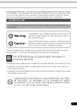
• For purposes of improvement, specifications and design are subject to change without notice.

• Please use this service manual 

when referring to the operating instructions without fail.

• Some illustrations used

 in this service manual are slightly different from the actual 

product.

Summary of Contents for NR1509

Page 1: ...ls marantz com NR1509 AP ZH index php Upload is planned for the time of a future press release BEFORE SERVICING THIS UNIT ELECTRICAL MECHANICAL REPAIR INFORMATION UPDATING Confidential Service Manual Ver 1 For purposes of improvement specifications and design are subject to change without notice Please use this service manual when referring to the operating instructions without fail Some illustrat...

Page 2: ...S ONLINE PARTS LIST Accessing the Parts List Searching Part Numbers or Ref Numbers NOTE FOR PARTS LIST SERIAL NUMBER Serial Number Organization SKU Code of this Unit POST SERVICE PRECAUTIONS Initializing this Unit JIG FOR SERVICING Before Servicing This Unit Electrical Mechanical Repair Information Updating 2 ...

Page 3: ...c diagrams and parts lists be sure to use the designated parts Be sure to mount parts and arrange the wires as they were originally placed For safety seasons some parts use tapes tubes or other insulating materials and some parts are mount ed away from the surface of printed circuit boards Care should also be taken with the positions of the wires by arranging them and using clamps to keep them awa...

Page 4: ...PUT CONDITION 4 CIRCUIT AND PARTS ARE SUBJECT TO CHANGE WITHOUT PRIOR NOTICE Electrostatic breakdown of the semi conductors or optical pickup may occur due to a potential differ ence caused by electrostatic charge during unpacking or repair work 1 Ground for Human Body Be sure to wear a grounding band 1 M ohm that is properly grounded to remove any static electricity that may be charged on the bod...

Page 5: ...mbers or Ref numbers 1 Enter the part number or Ref number in the search window of the Parts List and press the search button 2 The search results are displayed The name of the sheet in which the search part is used and the part s line are displayed 3 Next click the Sheet section of the search results 1 Parts indicated by nsp on this table cannot be supplied 2 When ordering a part make a clear dis...

Page 6: ...n The 14 digit serial number that contains the code of the manufacturing plant and the manufacturing date SKU code 14 digits Factory code Cumulative serial number Manufactured Year month The last 2digit of year Month 01 12 SKU Code of this Unit Before Servicing This Unit Electrical Mechanical Repair Information Updating 6 ...

Page 7: ... network related settings NOTE If the unit fails to enter the service mode in step 3 repeat the procedure from step 1 Initializing the device restores the customized settings to the factory settings Write down your settings in advance and reconfigure the settings after initialization Use the following jigs extension cable kit when repairing the PCBs Order with your dealer for the jigs your dealer ...

Page 8: ...P1 SCH20_AMP2 SCH21_SMPS SCH22_REG SCH23_FRONT CNT PRINTED CIRCUIT BOARDS DIGITAL F HDMI AV SPK SIDE CNT HDMI GUIDE A HDMI GUIDE B AMP FRONT MC HP USB REG GUIDE L FRONT CNT REG CNT SMPS LEVEL DIAGRAM FRONT ch CENTER ch SUBWOOFER ch SURROUND ch LEGO ADC BLOCK DIAGRAM ANALOG AUDIO DIAGRAM DIGITAL AUDIO DIAGRAM VIDEO DIAGRAM POWER DIAGRAM WIRING DIAGRAM SEMICONDUCTORS 1 IC s 2 FL DISPLAY 3 Remote Cod...

Page 9: ...LEGOVD17 LEGOVD19 LEGOVD20 LEGOVD21 LEGOVD22 LEGOVD8 LEGOVD10 MN864787_1 MN864787_1 MN864787_C CB05YTYH221 L1052 MN864787_C LEGOVD13 LEGOVD14 CB05YTYH221 L1053 LEGOVD0 LEGOVD2 LEGOVD5 LEGOVD7 LEGOVS LEGODE OPEN L1055 VDD33IO RX4_5V CEC_COM MN864787_2 MN864787_1 MN864787_0 MN864787_0 MN864787_C CEC3 3V CEC1 1V1 CEC5V D1035 OPEN D1034 OPEN D1022 OPEN D1021 OPEN RT1N441C Q1048 R1455 47K D1031 OPEN 47...

Page 10: ...R1673 R1486 OPEN 0 R1683 51 D 1608 R1513 1 4 2 3 R1501 0 2 1 4 2 3 R1497 0 2 OPEN 1005 D1064 OPEN 1005 D1066 LRB521S 30 D1078 D1079 LRB521S 30 OPEN 1005 D1070 OPEN 1005 D1068 C1627 100N K TX2 HDMI OUT 1 18 16 14 12 10 8 9 6 7 4 5 3 1 19 11 13 15 17 2 HPD4 CEC_COM RX5_5V RX4_5V CEC1 1V CEC5V RX5_DDCCL RX4_DDCCL RX5_2 RX5_2 RX5_1 RX5_0 RX5_C RX4_2 RX4_1 RX4_0 RX4_C RX4_C RX4_5V R1668 0 R1670 0 MN864...

Page 11: ...7623_C L1069 OPEN 2012 L1070 OPEN 2012 AIOS4_GPIO_SPI_EN_A R2113 0 R2107 33 R2108 33 R2109 33 100N K C1699 FB1005 CB05YTYH221 10U K 2012 C1693 P1TX1_0 P1TX1_1 P1TX1_2 R1645 10K P1TX1_C DGND FB1007 CB05YTYH221 R1618 OPEN R1624 OPEN ADV7623_SPI_CLK 10K R1632 C1687 OPEN 10K R1621 100 R1622 C1688 OPEN R1569 0 R1575 1M 4 2 1 3 X1005 28M63636 FA 238 R1623 1K D 1608 DV1 8V_1 DV3 3V_1 10U K 2012 C1702 1N ...

Page 12: ... DIR_DIN AP_CK RESET 10K R1176 100N K C1251 33 R1190 33 R1191 C1229 100N K DV_POWER1 DSP_FLAG0 RC_IN WAKE_UP TMS C1242 30P J E_RTS_MOEI E_RXD_MIEO TCK TU_IIC RDSI 33 R1173 OPEN R1178 C1230 100N K 33 R1189 CEC_OUT RXD_MI232O VEXP_DATA R1203 33 33 R1180 33 R1182 33 R1183 33 R1184 100 R1169 33 R1170 THERMAL_A THERMAL_E VEXP_STB M3 3V DGND VEXP_OE VEXP_DATA TU_DA THERMAL_E DSP_MISO HSDA DSP_ICS DSP_RS...

Page 13: ...00 C1213 100N K C1214 100N K R1114 100K VIN_A R1137 18K DCDET4 R1108 3K9 C1221 10N K R1118 100 R1140 OPEN R1121 120K HPD5 C1223 10N K R1122 100 10K F 1608 R1125 PTC1001 NCU18XH103J60RB VEXP_STB VEXP_CLK Q1058 2SC3052 HPD4 HPD2 R1135 100K R1098 100K C1216 100N K R1097 1K2 ADC_RST TXD_MO232I VEXP_DATA TO CPU THERMAL_E THERMAL_A VEXP_STB DCDET4 M3 3V DC_DET ASO Q1038 ISA1530AC1 22K R1099 2SC3052 Q102...

Page 14: ...RC_IN WAKE_UP PRE_MUTE KILL_IR MVOL_CLK TO CPU KEY2 ISEL_B VSEL_B RED_LED FL_RST FL_DA DIRECT_LED D1000 LRB521S 30 OPEN C1013 OPEN C1015 C1018 1N K C1017 1N K C1020 1N K N1003 C125Z2 27C N1002 C125Z2 17C FRONT_RL HI B_RL AMPSIGDET CURRENT_DET TU_DA TU_LA PRE_MUTE SEL_CLK DA 5V DAGND MVOL_MUTE MVOL_DATA MIC DACRTNGND THERMALDETE DC_DET4 THERMALDETA RLY_SB RLY_HIB COMPONENT SW1 COMPONENT SW2 COMP_CR...

Page 15: ...MCKI 33 R1915 33 R1914 DIR_RST DIRALRCKI DIR_CE R1953 10K DIR_CE TO CPU OPEN R1966 5 7 6 8 4 2 3 1 R1906 33 4 AR R1955 10K DV_POWER1 AP_DA TO DSP RX_SD2 RX_SD0 TXFS RX_BCLK R1988 100 R1987 100 R1983 100 R1934 100 DACDATAS DACDATAF DSP1INS SL R1942 100 DAC64FS R1933 100 R2005 100 DSP1IN_ FR DSP1IN_ SW DSP1IN_ SW R1936 33 DIRADATAI NET_TDM_DIN GPIO_0 DSP1INCSW C DSP1INCSW C R1927 100 DIRALRCKI GPIO_...

Page 16: ... 1N K C2119 1N K C2121 1N K C2118 2 2U M C2116 1N K C2123 1N K C2125 1N K C2127 1N K C2129 A DIN_L 1N K C2131 1N K C2133 1N K C2135 100N K C2196 C2198 220 25 KR3 R2058 100 1608 R2034 100 1608 R1999 100 1608 R2017 100 1608 C2146 OPEN 1608 OPEN 1608 C2154 C2137 OPEN 1608 100N K 1608 C2165 ADIN_LEGO_R PLDADCMCK PLDADCLRCK DA 5V DADATAF DA256FS FL FR CEN CEN C2201 220 25 KR3 SW C2202 100N K SL C2203 1...

Page 17: ...0 100N K MISO VCC GND 10K R1362 DSP1A3 DSP1A1 DSP1SDA10 DSP1A17 OPEN R1359 DSP1RAS DSP1CE0 DSP1CAS DSP1DQM DSP1D7 DSP1D6 DSP1D3 DSP1D2 R1342 33 4 AR DTMS DSP1D13 DSP1D12 DSP1D10 DSP1SDCLK DSP1D8 DSP1D6 DSP1D4 DSP1D1 DTRST DEMU0 10K R1351 DSP_FLAG0 C1431 1N K C1374 100N K C1451 100N K C1453 100N K C1370 100N K C1358 100N K 4K7 R1352 R1350 4K7 C1457 100N K TO DIR A PLD 1K2 R1396 SBL SBR FL FR DSP1MO...

Page 18: ...LK_2 NET3 3V AIOS4_SPI_MOSI_1 AIOS4_SPI_CLK_1 R1564 OPEN AIOS4_GPIO_SPI_EN_0 AIOS4_GPIO_SPI_CLK I2C_SDA AIOS4_GPIO_SPI_MOSI I2C_SCL AIOS4_GPIO_JTAG_TMS 7 5 3 1 4 6 2 8 9 10 N1022 RJ 45 JACK AIOS4_SPI_MOSI AIOS4_SPI_CLK GNDC RD TCT TD TD GND VBUS GPIO_2 GPIO_0 NET_TDM_DIN NET_TDM_FSIN NET_TDM_DOUT NET_I2S_LRCKOUT NET_I2S0_DOUT NET_I2S2_DIN NET_I2S2_DOUT NET_I2S2_BCKIN ETH_RX ETH_TX ETH_TX 0 2012 L1...

Page 19: ...EN 22U M 2012 C1850 22U M 2012 C1817 22U M 2012 C1881 C1858 OPEN C1856 OPEN 47 6 3 MVG C2109 1000P C1801 47 6 3 MVG C2194 OPEN C1802 R1816 0 2012 C1862 OPEN C1860 OPEN C1876 OPEN R1820 0 2012 C1868 OPEN C1864 OPEN C1870 OPEN C1872 OPEN C1874 OPEN C1871 OPEN C1873 OPEN C1875 OPEN 1U K 1608 C1807 1U K 1608 C1819 3 2 1 2SA2166 Q1066 R1777 10K 1U K 1608 C1792 C1945 OPEN C1946 OPEN C1944 OPEN C1949 OPE...

Page 20: ...D4014 LBAS16HT1G HIB_RL C4015 220 16 R4061 0 01 5 OPEN R4060 CLP4000 CLP4001 CLP4003 F4000A T6 3AL 250 V C4053 100N EB 100V JP4001 OPEN F4100A 7CH_AMP 2 2 N9 7CH_AMP 1 2 O5 7 6 5 4 2 3 1 CN4005 220MM 8P 4 3 1 2 6 5 7 8 9 10 11 12 13 CP4000 AMPSIGDET HIB_RL C S_RL HPRL C4062 100 16 VOLTAGE DETECT 47N M 50V C4006 L4006 SP 2507 47N M 50V C4005 R4004 10 1 5 L4004 SP 2507 C4010 47N M 50V R4002 10 1 5 L...

Page 21: ...DA_SR DAGND DA_SBL USB_R USB_L MVOL_CLK RETGND SEL_DATA TU_CK TU_IISD TU_IIC RDSI SEL_DATA MUTE_Z2 TU_IIC RDSI M DGND ZVOL_DATA Q4602 RT1N141C ZVOL_MUTE REMOTE3 3V 2 5 4 3 1 NC OUT GND IN ON OFF 10 50 C4710 3 1 4 2 N4600 1 0 11S 4PW FRONT IRIN R1456 1K C1344 4 7U K 1608 SHIELD COVER C1342 4 7U K 1608 N FB K OPTION TABLE R4637 33 TRIGGER REMOTE3 3V REG_CNT 1 4 B4 FROM WIRE CN4602 C125Z2 13 AV 1 3 H...

Page 22: ...OL_LATCH AGND R5302 2K2 AMP_FR AGND NR1609 MVOL_CLK AMP_SBL AMP_SL AMP_SR PRE_SW AMP_FR C5221 470 16 8 11 5 KR3 470 16 8 11 5 KR3 C5218 R5224 OPEN 270_1W LEGO_AD_R A 7V A 7V VIDEO SHEET PRE_SW2 OPEN R5239 180118 R5239 10K OPEN RLY_H P RLY_S C RLY_F H P_R H P_GND HIB_RL R5291 100K 100K R5292 DA_SBL DA_SBR C5215 100 16 PKR3 DA_SR C5213 100 16 PKR3 47 25_PKR3 DA_C NR1509 DA_FR R5212 0 SPK_SMPS 1 2 A9...

Page 23: ...PEN R5360 8K2 C5279 47N K C5282 1 50 C5283 47N K 1 3 5 7 9 11 13 15 17 18 20 19 21 4 2 6 8 10 12 14 16 CN5204 C125Z2 21C JK5200 CBL SAT OPTION_A C5301 1 50 C5300 1 50 C5298 1 50 C5296 1 50 C5294 1 50 COMP_SW2 C5278 100N K VINA SW2 NJM2595MTE1 V 5V VIN_C MUTE COMP_SW2 CR_OUT CB_OUT Y_OUT CN5402_21P DVD OPTION_B MODEL OPTION OPTION A R5377 75 C5289 68P J R5373 OPEN C5206 100N K INPUT SHEET 100 10 C5...

Page 24: ...1608 R5429 10K F 1608 C5327 CH 470P J 1608 R5407 4K7 F 1608 R4039 OPEN R4084 100K R5405 180 C4076 10 50 C5316 CH 680P J 1608 N1B N1SG ONLY 4K7 F 1608 R5471 A 8V 47K F 1608 R5463 4K7 F 1608 R5462 A 8V R5454 47K F 1608 R5453 4K7 F 1608 A 8V DAC OPTION 47K F 1608 R5445 4K7 F 1608 R5444 A 8V R5436 56K F 1608 C5329 CH 470P J 1608 A 8V 4K7 F 1608 R5426 R5417 4K7 F 1608 A 8V 47K F 1608 R5409 C5318 220 16...

Page 25: ...3016 10000N K 2012 TO DMAIN R3017 OPEN 3 6 4 7 5 1 2 10 12 8 11 9 23 22 20 19 21 16 18 17 15 13 14 6232 23P ST N3001 TX1_SHLD TX0_SHLD HPA_D DDC_SDA HDMI5V L3004 4 7UH 2012 CEC3 3V 4 7UH 2012 L3005 TX2_SHLD TXC_SHLD CE_REMOTE D3001 OPEN R3005 OPEN C3001 OPEN 2012 DDC_SCL CEC 4 3 1 2 L3003 OPEN CEC5V 4 7UH 2012 L3006 DGND3 4 3 1 2 L3002 OPEN 1 3 4 2 R3010 0 2 AR 1 3 4 2 R3009 0 2 AR 4 3 1 2 L3001 O...

Page 26: ...4451 100 1K R4449 Q4418 OPEN R4472 OPEN C4439 100P J GND DATA MICGND H PL H PR MICDET 560 R4453 BD4401 0 BD4400 0 BD4450 CB05YTYH221 2012 C4449 10 50 5 11 2K2 R4454 C4452 100N K LBAS16HT1G D4415 100N K C4460 D4416 D4417 OPEN GND DATA MIC LUG401 OPEN FROM TRANS UNIT 100 R4401 EC16B24T01D4ZZZ R4487 220K C4410 OPEN 100 R4422 R4421 100 Q4402 RT1N141C MICDET ZJ5 1B ZD4405 100 R4470 Q4417 RT1N141C USB_Y...

Page 27: ...PEN C4832 22 16 BKT4800 R4868 OPEN 7 4 5 6 2 3 1 8 CP4802 YMW025 08R 1 2 3 5 4 YMW025 05R CP4800 SPK_SMPS 1 2 O5 SPK_SMPS 1 2 A3 HDMI B D 18 21_K9 1K2 1 R4932 R4926 33K 390K R4925 C4824 OPEN 47 50_PKR3 C4816 R4908 22K R4902 47K TR_THERMAL 22K R4858 R4814 22K R4805 56K ASO_DET PRF18BG471QB5RB 65T NR1509 PRF18BF471QB5RB 75T NR1609 AV 1 3 O3 Q4825 KSA992F 1K2 R4916 R4894 100K R4882 33K R4881 390K Q48...

Page 28: ...ZD4809 150 R5094 2N2 K C4901 270 R5095 150 R5053 R5023 JUMPER 100P J C4852 R4973 1K2 1 1K2 R4936 R5091 220 D4830 OPEN C4884 100 50_PKR3 D4825 OPEN C4870 100 50_PKR3 D4820 OPEN KTC3206Y Q4864 R5082 33K KTC3206Y Q4855 3K3 1 R4963 47 1 R4974 R5005 OPEN R4964 OPEN 47 25_KOSHIN C4896 R5083 OPEN R5021 5K6 1 47 25_KOSHIN C4882 Q4833 KTC3964 R4937 5K6 1 22 1 R5028 22 1 R4987 OPEN C4874 0R22 2 R5076 2SB156...

Page 29: ...0 22 275V 0 22 275V 0 15 275V C4143 C4156 OPEN OPEN OPEN C4169 BKT4142 LINE_FILTER OPTION FUSE OPTION OPTION C4153 C4172 ZJ15B OPEN OPEN NR1509 OPTION_2 NR1609 OPTION DGND D5 2V TO HDMI B D TO POWER TRANS CHASSIS GND BKT4141 NR1509 1609 F4141 T6 3AL NR1509 1609 OPTION OPEN 1000P 1KV GRM31C7U3A102JW32L OPEN ZJ15B OPEN ZJ6 2B ZJ7 5B ZJ39B ZJ39B OPEN ZJ15B ZJ15B ZD4160 ZD4148 ZD4165 0 1 275V 2M2 5 2M...

Page 30: ...4600 KIA7805API D4634 OPEN 1N4148 D4607 OPEN ZD4601 D4608 OPEN 100N M 50V C4612 C4615 OPEN OPEN C4614 8V_IN AGND AGND AGND 8V_IN 5V_IN VGND 5V_IN F4603A D4617 1N4007S D4616 1N4007S 1N4007S D4625 D4624 1N4007S NR1609 FRONT CONNENCTOR REG_CNT 3 4 M7 JP4630 JUMPER 1 2 3 4 CN4607 CNT 4P C4602 10 50 D4600 1N4148 2 3 1 U4608 OPEN OPTION A D4611 OPEN 1 3 2 U4603 KIA7908PI D4610 OPEN 1 3 2 U4604 KIA7805AP...

Page 31: ...Y_HIB RLY_C S DA_ 5V CLP4600 H P_GND AGND AGND AD_VCOM LEGO_FR LEGO_FL CURRENT_DET RLY_HIB RLY_SB RLY_F H P_GND H P_GND AD_IN_R LEGO_FR AD_IN_L CLP4606 CLP4607 CLP4604 CLP4603 VIDEO 5V D MGND D MGND D MGND D MGND D MGND V IN C V IN A CURRENT_DET LEGO_VCOM INSERT CP4611_21P MODEL OPTION CP4613_23P OPEN CP4612_13P NR1609 CP4617_15P MODEL OPTION BKT4143 HDMI DIGITAL CNT E8 CLP4602 SC52136 041A MP SMP...

Page 32: ...M3 3V FL DCDET4 OPT SN74AHCU04PWR 30 PCM9211 AK4458VN ADSP21487KSWZ 120 TEST9 TEST8 5M570ZF256C5N TEST7 TEST6 TX64FS 22 5792MHz D SN74LVC244APWR D3 3V2 TC74VHC08FT CK F R5F5631FDDFB 40 120 140 80 60 MN864787 1 NC 160 SN74LVC244APWR 130 100 90 80 RESETOUT DGND 17PIN 27PIN 23PIN THERMALDETA SN74LVC244APWR 18 75MHz A VBUS RED 5V 15PIN 9 AMPSIG_DET 8 CURRENT_DET IN3 90 70 IN4 5V HPD ICT ADJ IN5 OUT MA...

Page 33: ...B 4 RLY_H P 23P TU_DA MIC_IN NJM8080 10 RC_5 CBL SAT_L Z2_L PRE_FL CB 19P DA_SBL RET_GND NJM8080 AMPSIG_DET D MGND COMPONENT_SW2 D MGND D MGND COMP_DET Blu ray CURRENT_DET D MGND COMPONENT_SW1 D MGND CBL SAT C5291 R5288 R5324 R5329 R5270 R4247 R4041 R5266 R5330 R5259 R5350 R4039 R5261 R5345 C4229 R4251 C5289 C5312 D5208 D5215 C5243 R5237 R5233 R5333 R5334 R5276 C5268 C5270 R5207 R5279 R5476 R5478 ...

Page 34: ...8 JS4009 R1456 J S 4 0 11 Q4604 U4700 JS4010 AGND AGND A 7V 14 KILLIR 16 RC_OUT 12 RC_IN 11 MUTE3 3V 2 M DGND 3 ZVOL_MUTE 1 RC 5 5 ZVOL_CLK 6 TU_IISD 7 TU_DA 8 TU_CK 9 TU_LA 7 TRG1 11 SEL_CLK 12 SEL_DATA 13 RETGND 14 RETGND 15 MVOL_MUTE 17 MVOL_DATA 18 MICGND 19 MIC_IN 20 MICGND 21 USB_R 2 DA_SBR 3 DAGND 4 DA_SBL 5 DA_SBL 1 DA_SBR 8 DA_SR 10 DA_SL 11 DA_SL 9 DAGND 7 DA_SR 14 DA_SW 15 DAGND 16 DA_C...

Page 35: ...30 R5046 R5026 R5083 R5071 C4894 R4811 Q4801 R5098 R4824 C4811 C4801 R4805 Q4830 R4952 D4817 D4812 R5001 R4997 R4873 R4868 C4866 C4873 R4986 R4856 D4829 R5027 D4832 C4804 D4809 D4810 C4880 D4835 C4800 R4804 R4815 R4820 D4802 R4944 R4948 C4859 C4852 D4819 R4919 C4835 R4897 R4904 R4907 R4911 C4863 R4979 R4989 C4815 R4848 R5042 R5020 C4892 R5075 R4891 R4828 D4800 Q4804 R4818 R4823 R4832 R4950 Q4832 R...

Page 36: ...G_B D_MP 11P TRG GND 9P 9P 7908 7020 08223 000 0S Pb 4 AGND 5 AGND 6 A 8V 7 A 8V AGND AGND AGND AGND AGND 8V_IN 3 TU5V 5V_IN 5V_IN TRG GND 5V_IN 5V_IN TRG 15V TRG 15V VGND VGND VIDEO 5V VIDEO 5V 11 TRG 15V 8 DA_ 5V 1 RL_GND 2 RL_ B 8V_IN 8V_IN 8V_IN VIDEO_GND VIDEO_GND 9 TRG GND 10 TRG GND R5366 Pb R5373 R5379 R5381 C5294 C5297 R5377 R5369 R5372 R5378 C5293 R5368 C5298 R5367 R5374 C5292 R5365 C529...

Page 37: ...dB SW NONE DIGITAL 2 0dB 0 5dB 12dB 9 5dB SW NONE ANALOG 2 0dB 12dB 3 0dB 13 0dB Basic OFFSET of VOL 0dB Fine tuning by Digital input OFFSET of SW NON OFFSET of the AD input 2 0 0 5 12 9 5dB 2 0 12 3 13 0dB 0 4dB SW NO 32dBFS DIG IN 35 0dBFS A D IN 20dBFS DIG IN 23 0dBFS A D IN 0dBFS 10dBFS 20dBFS 30dBFS 40dBFS AK4458 0 4dB Differential Out NJU72343 MAX OUTPUT 4 2Vrms LINE IN H POUT SPEAKER OUT DS...

Page 38: ... LIMIT LEVEL ALLch 3dBFS 0dBFS 10dBFS 20dBFS 30dBFS 40dBFS AK4458 0 4dB Differential Out NJU72343 MAX OUTPUT 4 2Vrms SPEAKER OUT DSP GAIN ADJ AK4458VN D A PLD NJU72343 PREOUT DD INPUT 20dBFS 1kHz DSP OUTPUT 20dBFS ANALOG INPUT 200mVrms L R 1kHz MODE MULTI CH STEREO DSP OUTPUT 23 0dBFS PREOUT 159mVrms Before Servicing This Unit Electrical Mechanical Repair Information Updating 38 ...

Page 39: ... 40dBFS DIG IN DD Config1 INPUT 30dBFS DD LFE 34dBFS PCM IN 37dBFS A D IN INPUT 20dBFS DIG IN PCM 200mV A D IN 6 5dB MGAIN setting of MASTER VOL 00dB DOLBY DIGITAL IN 2 0dB 0 5dB 14dB 11 5dB PCM DIGITAL IN 2 0dB 0 5dB 14dB 11 5dB ANALOG IN 2 0dB 14dB 3 0dB 15 0dB Basic OFFSET of VOL 0dB Fine tuning by Digital input OFFSET of SW ch OFFSET of A D input 2 0 0 5 14 11 5dB PREOUT 300mVrms 0dBFS 2 8Vpp ...

Page 40: ...BY LIMIT LEVEL ALLch 3dBFS 0dBFS 10dBFS 20dBFS 30dBFS 40dBFS AK4458 3 4dB Differential Out NJU72343 MAX OUTPUT 4 2Vrms SPEAKER OUT DSP GAIN ADJ AK4458VN D A PLD NJU72343 PREOUT DD INPUT 20dBFS 1kHz DSP OUTPUT 23dBFS ANALOG INPUT 200mVrms L R 1kHz MODE MULTI CH STEREO DSP OUTPUT 26 0dBFS PREOUT 159mVrms Before Servicing This Unit Electrical Mechanical Repair Information Updating 40 ...

Page 41: ...dB 20dB 10dB 0dB 20dB 30dB 40dB 10dB LINE IN 200mV 30dB LINE IN NJU72750 To MAIN 8 5dB 10dBFS 0dBFS 1 06Vrms 20dBFS 30dBFS 40dBFS A D IN 75 2mVrms 23 0dBFS PCM9211 PCM9211 A D To LEGO To ZONE2 Before Servicing This Unit Electrical Mechanical Repair Information Updating 41 ...

Page 42: ...R ALL MODEL FM AM MIC Mini Jack TUNER_R BUFFER BUFFER 8 CH VOLUME NJU72343 2 2ch PREOUT PRE FR PRE FL OutD InH2 InH1 InG2 InG1 InF InE InD InC InB2 InA2 OutH OutG OutF OutE OutC InA1 OutA InB1 OutB Control Logic 8 CH VOLUME NJU72343 TO DIGITAL AUDIO BLOCK TO DIGITAL AUDIO BLOCK 7 INPUT 3 OUT NJU72750 HEADPHONE OUT OutB3 OutA2 OutA1 OutB2 OutB1 OutA3 InB6 InB5 InB2 InB1 InA7 InA4 InA3 InB4 InB7 InB...

Page 43: ...IR1 DATADIR1 SLRCK LEGO_L DAC_64FS DACDATAF DA C DA FL DACDATAS DA SR DA SL ADIN_R ADIN_L LEGO_SPDIF LEGO_I2S SLRCK FSDIR1 256FSDIR1 DIRADATAI DIRABCKI DIRAMCKI INA DATAS DATAF DSP1OUTMCK DSP1OUT64FS DSP1INCSW DSP1INF DSP1INFS DSP1INMCK HDMI OUT1 USB FRONT ADV8195 TMDS BUFFER PCM9211 DIR A D DATADIR1 SBCK MCLK1 DIRALRCKI 64FSDIR1 ADV7623 HDMI TRANSCEIVER DATAC DSP1OUTFS DSP1INS DSP1INSB DSP1IN64FS...

Page 44: ...DDR2RAM RJ 45 Ethernet Transceiver ADV8195 BUFFER HDMI3 HDMI2 HDMI1 HDMI5 u COM CON IC CON CVBS INPUT SW 6dB 6dB 24bit RGB Data CLK Vsync Hsync Data Enable 24bit RGB Data 480P 59 94Hz 576P 50Hz TTL REC656 INãÁ 480P TMDS IN 4K 60 50HZ 6Gbps TMDS IN 4K 60 50HZ 6Gbps BLU RAY CBL SAT MUTE OPEN OUT0 ADV7623 HDMI TRANSCEIVER in3 in0 MX25L3206EM2I 4K GUI TMDS OUTPUT OUT1 CVBS IN LEGO MODULE 6 5 4 2 3 1 G...

Page 45: ...mA 25mA 55 8mA 24mA 50mA 409 8mA CEC_POWER2 DV_POWER1 CPU_POWER AC CORD VCC TPS563200 DV1 8V TPS563200 DA1 1V TPS563200 D3 3V KIA7908API KIA7808API TPS22975 LEGO_5V TPS22975 DA_3 3V TPS22975 CEC_3 3V CEC_POWER2 FL5V P DIRECT LED VOLTAGE DA 3 3V AK5358BET AP7361_ADJ MAIN TRANS CEC1 1V HDMI RX TX MN864787 MN864788 DA1 1V DSP ADSP21487KSWZ 2B DV1 8V ADV7623 5M570ZF256C5N DV3 3V ADV7623 MX25L3206EM2I ...

Page 46: ... PLATE 4P FRONT PCB 7CH AMP PCB SMPS PCB H P MIC PCB USB PCB FRONT HDMI PCB MAIN SPK PCB DIGITAL PCB FRONT CNT PCB AV PCB REG CNT PCB REG PCB SIDE CNT PCB WiFi_ANT WiFi BT_ANT Before Servicing This Unit Electrical Mechanical Repair Information Updating 46 ...

Page 47: ...RC_IN I M3VPu I I I Remote input 27 P32 TXD6 TXD0 IRQ2 DS BDOWN I M3VPu I I I Detect power down 28 TMS P31 IRQ1 DS TMS NC NORMRAL I I M3VPu I I I E20 Emulator control pin When normal operating mode set to input 29 TDI P30 RXD1 IRQ0 DS TDI RXD_MIT SUBISHI I O I M3VPu I I I E20 Emulator control pin Mitsubishi writter control pin When normal operating mode set to input 30 TCK FINEC P27 TCK NC NORMRAL...

Page 48: ...5 VSS VSS Ground pin 106 PE5 IRQ5 AN3 KEY1 I M3VPu I I I Key control signalinput pin When standby mode set to inturrupt 107 PE4 AN2 DC_DET ASO I SW3VPu I I I Protection detect signal input pin for DC and ASO A D converter Pin Pin Name Symbol I O Pu Pd STBY STOP CEC STBY Function 108 PE3 AN1 AMPSIGDET I Pd I L I Signal level monitor pin AD converter 109 PE2 RXD12 IRQ7 DS AN0 CURRENT_DET I Pd I L I ...

Page 49: ...CTIONAL AD8195 SCL_IN SDA_IN SCL_OUT SDA_OUT CEC_IN CEC_OUT PCM9211 DIGITAL U1040 PIN Functions PIN DESCRIPTION NO NAME I O 5 V TOLERANT 1 ERROR INT0 O No DIR Error detection output Interrupt0 output 2 NPCM INT1 O No DIR Non PCM detection output Interrupt1 output 3 MPIO_A0 I O Yes Multipurpose I O Group A 1 4 MPIO_A1 I O Yes Multipurpose I O Group A 1 5 MPIO_A2 I O Yes Multipurpose I O Group A 1 6...

Page 50: ...nboard pull down resistor 50 k Ω typical 5 CMOS Schmitt trigger input PCM9211 BLOCK DIAGRAM Clock Data Recovery MPIO_A SELECTOR MPIO_C SELECTOR MPIO _B SELECTOR ADC Com Supply MPO0 1 SELECTOR MPO 0 MPO 1 MAIN OUTPUT SCKO BCK LRCK DOUT PORT RXIN8 RXIN9 RXIN10 RXIN11 DITOUT AUTO DIR ADC AUXIN0 AUXIN1 AUXIN2 AUTO DIR ADC AUXIN0 AUXIN1 AUXIN2 AUTO DIR ADC AUXIN0 AUXIN1 DIT Lock DIR Unlock ADC AUXIN 2 ...

Page 51: ... PIN CONFIGURATION 54 53 52 51 50 49 48 47 46 45 44 43 42 41 40 39 38 37 36 35 34 33 32 31 30 29 28 1 2 3 4 5 6 7 8 9 10 11 12 13 14 15 16 17 18 19 20 21 22 23 24 25 26 27 DQ0 DQ1 DQ2 DQ3 DQ4 DQ5 DQ6 DQ7 LDQM CAS RAS CS BS0 BS1 A10 AP A0 A1 A2 A3 DQ15 DQ14 DQ13 DQ12 DQ11 DQ10 DQ9 DQ8 NC UDQM CL K CKE NC A11 A9 A8 A7 A6 A5 A4 VDDQ VDDQ VSSQ VSSQ VDD VDD VSS VSSQ VSSQ VDDQ VSS VSS WE VDD VDDQ W9864G...

Page 52: ...n PCM mode 100k Ω Pull down DSDL3 I Audio Serial Data Input in DSD mode TDMO2 O Audio Serial Data Output in Daisy Chain mode 8 DSDR3 I Audio Serial Data Input in DSD mode Hi Z 9 DSDL4 I Audio Serial Data Input in DSD mode Hi Z 10 DSDR4 I Audio Serial Data Input in DSD mode Hi Z 11 DZF O Zero Input Detect in I2C Bus or 3 wire serial control mode 100k Ω Pull down SMUTE I Soft Mute Pin in Parallel co...

Page 53: ... 41 VREFL4 I Negative Voltage Reference Input Pin AVSS Hi Z 42 AOUTR4N O Rch Negative Analog Output 4 Pin Hi Z 43 AOUTR4P O Rch Positive Analog Output 4 Pin Hi Z 44 LDOE I Internal LDO Enable Pin L Disable H Enable Hi Z 45 TVDD Digital Power Supply Pin 3 0V 3 6V 46 DVSS Digital Ground Pin 47 VDD18 O LDO Output Pin LDOE pin H This pin should be connected to DVSS with 1 0µF Note 4 I 1 8V Power Input...

Page 54: ...CK IC control clock input 3 InB1 Bch input1 19 NC 4 InA2 Ach input2 20 NC 5 InB2 Bch input2 21 OutB3 Bch output3 6 InA3 Ach input3 22 OutA3 Ach output3 7 InB3 Bch input3 23 REF_B Bch reference potential terminal 8 InA4 Ach input4 24 OutB2 Bch output2 9 InB4 Bch input4 25 OutA2 Ach output2 10 InA5 Ach input5 26 REF_A Ach reference potential terminal 11 InB5 Bch input5 27 OutB1 Bch output1 12 InA6 A...

Page 55: ...3 13 13 13 13 13 13 13 13 13 13 2b SEGA14 14 14 14 14 14 14 14 14 14 14 14 14 14 14 14 14 3a SEGA15 15 15 15 15 15 15 15 15 15 15 15 15 15 15 15 15 2a SEGA16 16 16 16 16 16 16 16 16 16 16 16 16 16 16 16 16 Dp SEGA17 17 17 17 17 17 17 17 17 17 17 17 17 17 17 17 17 SEGA18 18 18 18 18 18 18 18 18 18 18 18 18 18 18 18 18 1d SEGA19 19 19 19 19 19 19 19 19 19 19 19 19 19 19 19 19 1e SEGA20 20 20 20 20 2...

Page 56: ... Movie Video Mode Game 16 84 53 16 84 53 RCRC51608453 X Select Video Mode Game HDMI Output Select Toggle 16 120 00 16 120 00 RCRC51612000 HDMI Output select 1 2 Toggle SR8001 from MZ02xxxxxxxxxx HDMI Out 1 16 120 01 16 120 01 RCRC51612001 HDMI Output 1 select SR8001 later S N MZ02xxxxxxxxxx HDMI Out 2 16 120 02 16 120 02 RCRC51612002 HDMI Output 2 select SR8001 later S N MZ02xxxxxxxxxx HDMI Out Au...

Page 57: ...M 17 46 17 46 RCRC517046 X X Select AM for Tuner 1 T MODE 17 37 17 37 RCRC517037 X X Tuning mode Auto or Manual for Tuner 1 MEMO MEMORY 17 41 17 41 RCRC517041 X X Memory for Tuner 1 HD Radio Tuner MEMORY 24 41 50 24 41 50 RCRC52404150 X X Enter Preset memory mode Store FREQ tuning Up 17 30 17 30 RCRC517030 X X Frequency Scan up for Tuner 1 FREQ tuning Down 17 31 17 31 RCRC517031 X X Frequency Scan...

Page 58: ...lect Main Zone Source Cal USB 16 92 11 16 92 11 RCRC51609211 Select USB input directly Blu ray BD 16 92 12 16 92 12 RCRC51609212 Turn On and select BD M XPort 16 92 13 16 92 13 RCRC51609213 Turn On and select M XPort Game 16 92 14 16 92 14 RCRC51609214 Turn On and select Game PHONO 16 92 15 16 92 15 RCRC51609215 Turn On and select Phonon Bluetooth 16 92 16 16 92 16 RCRC51609216 Turn On and select ...

Page 59: ...IN input was used These commands are recognized as for Main room zone commands when they are received via Front IR receiver or Rear Remote Control In These commands are recognized as for Multi room zone commands when they are received via Rear Multi room Remote In 2 Need an input assign to the input in Menu in advance the use 4 U1x version for North America model only 5 N1x version for Europe mode...

Page 60: ...MBLY Flowchart 1 FRONT PANEL ASSY 2 RADIATOR ASSY 3 DIGITAL PCB 4 SPK PCB 5 TRANS 6 SMPS PCB 7 REG PCB 8 AV PCB EXPLODED VIEW PACKAGING VIEW Before Servicing This Unit Electrical Mechanical Repair Information Updating 60 ...

Page 61: ...RANS DISASSEMBLY 5 TRANS and EXPLODED VIEW POWER TRANS Ref No of EXPLODED VIEW 24 RADIATOR ASSY DISASSEMBLY 2 RADIATOR ASSY and EXPLODED VIEW AMP PCB Ref No of EXPLODED VIEW P 8 GUIDE L PCB Ref No of EXPLODED VIEW P 7 DIGITAL PCB DISASSEMBLY 3 DIGITAL PCB and EXPLODED VIEW DIGITAL PCB Ref No of EXPLODED VIEW P 16 NETWORK MODULE Ref No of EXPLODED VIEW P 17 SPK PCB DISASSEMBLY 4 SPK PCB and EXPLODE...

Page 62: ...ting direction X View from the top Attention When reinserting the Antenna Cable after it has been disconnected make sure it is facing the direction shown in A above Shooting direction C Shooting direction D Shooting direction A Shooting direction B Glue x2 GASKET Proceeding TOP COVER FRONT PANEL ASSY 1 Remove the screws 2 Remove the screws Remove the CORD HOLDER and connectors Remove the FFC 1 FRO...

Page 63: ...2 x1 CP4401 FFC N1021 N1006 FFC CUT CORD HOLDER CP4801 CP4800 CP4802 CORD HOLDER Proceeding TOP COVER DIGITAL PCB 1 Remove the screws 2 Cut the wire clamps then remove the CORD HOLDERs and connectors Remove the FFC 3 Remove the connector 3 DIGITAL PCB Shooting direction A x2 x6 x1 FFC N1021 N1006 FFC CUT N1033 CORD HOLDER CUT N1005 N1007 N1001 N1003 N1002 Before Servicing This Unit Electrical Mech...

Page 64: ...ews NOTE It will separate and TRANS will fall from SET if screws is removed Proceeding TOP COVER SMPS PCB See EXPLODED VIEW for instructions on removing the SMPS PCB Proceeding TOP COVER REG PCB See EXPLODED VIEW for instructions on removing the REG PCB Proceeding TOP COVER DIGITAL PCB AV PCB See EXPLODED VIEW for instructions on removing the AV PCB 5 TRANS CP4001 from CP4401 CP4607 CP4142 CORD HO...

Page 65: ... P15 8 P8 1 P16 1 P12 2 P15 2 36 A 2 A 3 A 4 A 2 A 3 A 4 A 1 S5 21 S2 10 S15 1 S16 4 S2 7 S12 4 S7 6 S9 2 S4 4 S8 2 S2 1 S11 1 S2 1 S2 2 S2 1 S14 2 S8 11 S2 1 S2 2 S8 2 S1 2 S10 1 S2 2 S1 S15 2 S2 1 S2 1 S13 1 S2 2 S2 7 S3 1 S6 1 S11 4 S11 2 NR1609 NR1509 S1 1 23 NR1609 17 NR1509 S2 1 X2 S13 8 NR1609 6 NR1509 NR1509 1609 Marantz EXPLODE VIEW NR1509 Only z z Ref No 42 See PROCEDURE AFTER REPLACING ...

Page 66: ...pper bag are supplide CARD PASS K only WIFI ANTENNA FLY SHEET 128 x 91mm WIFI ANTENNA 2 pcs FM Antenna AM Antenna Antenna Isolator K only POLY BAG PACKING STYLE 13 10 NR1603 11 FB FB NR1609 11 FB NR1609 11 FB NR1501 13 FB NR1501 BOX BOTTOM TAPE O BOX BOTTOM CLIP X 1 SET FRONT SET FRONT SET FRONT 14 15 6 2 3 5 4 12 9 F AND K ONLY HERE CORD AC S E T TAPE Yellow 16 31 20 18 17 19 8 21 22 23 26 27 30 ...

Page 67: ... IN DIGITAL BLOCK SPECIAL MODE Special mode setting button 1 Version Display Mode 2 PANEL REMOTE LOCK Selection Mode 3 1 Selecting the Mode for Service related 3 2 Protection History Display Mode 3 3 Operation Info Mode 3 4 TUNER STEP mode U N only 4 Protection Pass Mode 5 Network Initialization Mode 6 Clearing the Operation Info 7 Log Capture feature DIAGNOSTIC MODE Service Path Check Mode DIAGNO...

Page 68: ...hat connect the PCBs Is DC5V output even when the connector N1033 supplying power from the SMPS PCB to the DIGI TAL PCB is removed Check the circuits around the Microproces sor on the DIGITAL PCB and replace any faulty parts Check for breakages and short circuits in the cir cuits and parts between N1033 on the DIGITAL PCB and the microprocessor power supply and replace any faulty parts Connect the...

Page 69: ...47 R2062 C1785 C1794 C1810 C1885 R2015 TPS563200 U1067 N1005 N1015 FL ASODET COAX TRG1 DAC_SBR B DCDET3 DA3 3V 90 80 60 70 2 2U 100 40 MPO0 MPO1 A DGND 110 20 130 10 TXI2S0 TXFS DGND GND GND DGND TCT G B VBUS D F LEGO5V 3 3U NET3 3V D3 3V2 90 80 70 CK G GUI_WRITE NET3 3V_POWER 60 IN1 130 140 50 DA 20 30 10MHz RES IN2 12 NC 14 RLY_F 10 RLY_HIB 11 RLY_H P 13 RLY_C S 15 DA 5V 2 D MGND 3 NC 4 NC 5 VIN...

Page 70: ...fer ent Blu ray DVD player is used The Blu ray DVD player is faulty NO NO YES YES YES YES NO NO YES YES YES NO NO NO No picture or sound is output Check the Blu ray DVD player Check the connection of the HDMI DVI cable 1 Is the HDMI DVI cable correctly inserted 3 Is a certified HDMI cable with the HDMI mark being used 4 Is the HDMI DVI cable shorter than 5m 5 When the input signal is Deep Color or...

Page 71: ...re a picture and sound output when a differ ent TV is used Check the unit The TV is faulty See HDMI Rx Tx Failure Detection YES NO Before Servicing This Unit Electrical Mechanical Repair Information Updating 71 ...

Page 72: ...or dts CHECK 4 INPUT SURROUND MODE SOURCE Audio output OK HDMI Legacy PCM2ch or DolbyDigital or dts CHECK 6 INPUT Connect AVR s connected in HDMI audio out put OK HDMI This unit s HDMI OUT Other AVR s HDMI IN Setting SURROUND MODE SOURCE CEC STANDBY HBR audio DolbyTrueHD or dtsHD MA CHECK 5 INPUT SURROUND MODE SOURCE Audio output OK HDMI HBR audio DolbyTrueHD or dtsHD MA CHECK 3 INPUT SURROUND MOD...

Page 73: ... resistor Replace the emitter resistor Replace the base resistor Replace the trimmer potentiometers Connect the connectors correctly Repair the DIGITAL PCB 4 3 Analog audio No audio output Is a voltage of 8 V supplied to AV PCB CP5201 Is there an audio signal in AV PCB CN5203 Reconnect the connectors correctly If the malfunctioning channel and function can be identified check the corresponding sig...

Page 74: ... turn on the power again Check the connection environment Checking the unit Can the output voltage 5V to Q1083 FET SW be confirmed Can the voltage 5V be confirmed between N1033 2 5pin Is NET5V POWER U1013 40pin uCOM Hi The circuit of NET5V POWER between U1013 Q1083 FET SW are faulty The circuit around Q1083 FET SW is faulty The circuit between the AC inlet and N1033 is faulty Check the SMPS PCB Ca...

Page 75: ...le inserted correctly into Net work Module Is the Bluetooth device compatible with the A2DP profile Is the Bluetooth function enabled on the Blue tooth device Connect the antenna cable correctly Use a device that is A2DP profile compatible Enable the Bluetooth function and try connecting again 5 2 Cannot establish a Bluetooth connection Checking the unit Check the Bluetooth device being used YES N...

Page 76: ...onnect the connectors correctly 5 3 Cannot recognize the connected USB device Checking the unit If no picture is output Check the VIDEO circuit Are digital video signals LEGOPCK LEGOVS LEGOHS LEGODE LEGOVD0 LEGOVD23 output from Network Module to U1024 MN864787 Checking the unit If no sound is output Check the U1021 DSP AUDIO circuit and the circuits thereafter Are the I2S signal output to U1008 7 ...

Page 77: ...A VBUS RED 5V 15PIN 9 AMPSIG_DET 8 CURRENT_DET IN3 90 70 IN4 5V HPD ICT ADJ IN5 OUT MAIN_PWR RC_IN WAKE_UP MUTE3 3V SWM3 3V TXD_MO232I RXD_MI232O ZVOL_MUTE ZVOL_DATA ZVOL_CLK MUTE_Z2 DAC_SBR DAC_SBL DAC_SBL 15PIN MN864788 Antenna Cable 7020 08228 000 0S NR1509 DIGITAL MP U1013 U1021 U1041 U1024 Q1080 N1021 U1008 R1995 N1033 U1067 R1805 C1922 R2119 C2121 C2110 C2115 C2117 C1873 C1361 C1375 C1377 C1...

Page 78: ...B Are any parts damaged Replace the U4140 TOP268VG and D4142 D4143 D4144 D4145 DC 5V is not output NO NO NO YES YES YES YES YES YES 1 3 2 OPTION OPTION OPTION OPTION OPTION BKT4142 OPTION_2 OPTION EER2525 T4140 TOP268VG IC_TOP268VG U4140 S V S S X C S S F S D A B C After primary side rectification Caution High voltage electric shock Primary drain Caution High voltage electric shock After secondary ...

Page 79: ... for deformed pins OK NG Check by following the flow chart for 3 Starting detecting the point of failure NOTE After checking troubleshooting 3 HDMI DVI check 3 Starting detecting the point of failure Replace the HDMI connector HDMI Rx Tx Failure Detection 1 Prior checking Before Servicing This Unit Electrical Mechanical Repair Information Updating 79 ...

Page 80: ...of flexible card cable Using the 7P FFC Straight is 1PIN side 4P FFC Cabele WRITING KIT RS 232C Cable S706 709 No Preference S702 3 3V 6 3 7 1 5 5 2 a 2 b Figure 1 Device Connection Method NR1509 2 Preparations for checking HDMI Switcher reception transmission register 2 3 Device configuration method PC settings Execute the serial communication program Termite exe The serial port setup screen will ...

Page 81: ...p Assistant execute the above Display changes Figure 4 Change of the Display of the Communication Start Button Name Press Figure 6 1 AVR settings NR1509 All the indicator Lights for Volume 7 segment Figure 6 FLD Display When Set When the settings are correct the following message will be displayed in the window of Termite 00 Start Sub CPU Log Mode is a version of Sub CPU The setup is now complete ...

Page 82: ...de table items Error Code table Error Code Check item No Description H1 01 Check item 5 Communication Error with HDMI RX Tx U1027 MN864788 H1 02 Check item 10 Communication Error with HDMI SW U1024 MN864787 H1 07 Check item 12 Communication Error with OSD U1030 ADV7623 H1 08 Check item 19 Communication Error with DSP U1021 ADSP21487 H1 12 Check item 24 Communication Error with DIR U1040 PCM9211 H1...

Page 83: ...onnected to the HDMI input terminals in order are the images on the player displayed on the TV in both cases HDMI OUT1 HDMI IN1 Check item 3 Check operation of the HDMI output terminal When the SETUP button on a remote control is pressed is MENU displayed on TV which is connected to the HDMI out put terminal on the AVR Is the DIG indicator illuminated on the FLD When the DIG indicator is illuminat...

Page 84: ...th a new device The power supply circuit is faulty Replace the PCB Recheck from check item 1 If it does not work replace the PCB 3 1 Error Code H1 01 failure detection procedure NO NO YES Go to next page Checking the reset waveform HDMI Rx Tx Check item 7 Checking the reset waveform Check the waveform When the power is turned on is the TP waveform correct as shown in the figure U1027 115 pin Check...

Page 85: ...CB Check item 9 Check the I2C commu nication line Check HDMI Rx Tx U1027 CPU U1013 patterns as well as soldering If there is no problem go to the next step Check the HDMI SW Remove the damping resistor R1974 R1975 of U1024 Is the I2C waveform correct Recheck from check item 1 If it does not work replace the PCB Check the HDMI Rx Tx Remove the damping resistor R1537 R1538 of U1027 Is the I2C wavefo...

Page 86: ...rcuit between CPU U1013 and HDMI SW U1024 If there is no problem the HDMI SW U1024 is faulty Replace with a new device NO Examples of confirmation waveform Voltage scale 1 0V div Time scale 20ms div Check item 11 Checking the HDMI SW Remove the R1974 R1975 Is the waveform of I2C the correct waveform HDMI SW U1024 is faulty Replace with a new device Recheck from check item 1 If it does not work rep...

Page 87: ... 3 3 Error Code H1 07 failure detection procedure NO HDMI OSD U1030 is faulty Replace with a new device Recheck from check item 1 If it does not work replace the PCB The power supply circuit is faulty Replace the PCB NO YES YES Check item 14 Checking the reset Check the CPU When the power is turned on is the TP waveform correct as shown in the figure U1030 97 pin Checking the reset waveform Exampl...

Page 88: ...esistor R1622 R1606 of U1030 Is the I2C waveform correct The CPU U1013 is faulty Replace with a new device Check the I2C communication line Recheck from check item 1 If it does not work replace the PCB OSD U1030 is faulty Replace with a new device YES The diagram shows an example Signal patterns vary depending on the timing Points for checking waveforms Crest value 3 3V normally Signal change SCL ...

Page 89: ...Write to the OSD ROM Recheck from check item 1 Does Error Code H1 15 continue Check item 18 Replace U1029 with a new device Recheck from check item 1 Does Error Code H1 15 continue Go to check item 12 Recheck from check item 2 YES YES NO NO Before Servicing This Unit Electrical Mechanical Repair Information Updating 89 ...

Page 90: ...o to next page 3 5 Error Code H1 08 failure detection procedure NO DSP U1021 is faulty Replace with a new device Recheck from check item 1 If it does not work replace the PCB The power supply circuit is faulty Replace the PCB NO YES YES Check item 21 Checking the reset Check the CPU When the power is turned on is the TP waveform correct as shown in the figure U1021 Q1040 Checking the reset wavefor...

Page 91: ...ns as well as soldering If there is no problem go to the next step Check the SPI communication line DSP U1021 is faulty Replace with a new device YES The diagram shows an example Signal patterns vary depending on the timing Points for checking waveforms Crest value 3 3V normally Signal change CLOCK frequency about 6MHz Voltage scale 2 0V div Time scale 2us div NO YES Recheck from check item 1 If i...

Page 92: ...6 Error Code H1 12 failure detection procedure NO DIR U1040 is faulty Replace with a new device Recheck from check item 1 If it does not work replace the PCB The power supply circuit is faulty Replace the PCB NO YES YES Check item 26 Checking the reset Check the CPU When the power is turned on is the DIR U1040 34pin waveform correct as shown in the figure U1040 34 pin Checking the reset waveform R...

Page 93: ...s as well as soldering If there is no problem go to the next step Check the communication line DIR U1040 is faulty Replace with a new device YES The diagram shows an example Signal patterns vary depending on the timing Points for checking waveforms Crest value 3 3V normally Signal change CLOCK frequency about 2MHz Voltage scale 2 0V div Time scale 2us div NO YES Recheck from check item 1 If it doe...

Page 94: ...nch destination according to the value returned Example i 0006 00FF 0001 HDMI in 4 5 00 Detection of 5V is not OK 00 or 04 Detection of DDC is not OK 22 Detection of DDC is OK HDMI In4 22 or 20 HDMI In5 11 or 10 Detection of 5V is OK Go to check item 31 Go to check item 32 Go to check item 33 Check item 30 Checking the DDC status register Send the following command from Termite exe Case of HDMI IN...

Page 95: ...heck item 2 If it does not work replace the PCB HDMI Rx Tx U1027 is faulty Replace with a new device Check for a short circuit in the 5 V line and the 5 V Switch IC U1025 If there is no problem the HDMI Rx Tx U1027 or the 5 V Switch IC U1025 is faulty Replace with a new device Check for a short circuit in the DDC line If there is no problem the HDMI Rx Tx U1027 is faulty Replace with a new device ...

Page 96: ...llowing test point Is the waveform like the sample HDMI In4 80 81 83 84 86 87 89 90pin HDMI In5 93 94 96 97 99 100 102 103pin U1027 Checking the TMDS status register Example i 0006 00FF 0001 Check for a short circuit in the pattern of the TMDS line of the HDMI Rx Tx U1027 from the HDMI input terminal If there is no problem the HDMI Rx Tx U1027 is faulty Replace with a new device HDMI Rx Tx U1027 i...

Page 97: ...In2 In3 00 Detection of 5V is not OK 00 or 04 Detection of DDC is not OK 22 Detection of DDC is OK HDMI In1 44 or 40 HDMI In2 22 or 20 HDMI In3 11 or 10 Detection of 5V is OK Go to check item 38 Go to check item 39 Go to check item 40 Check item 37 Checking the DDC status register Send the following command from Termite exe Case of HDMI IN1 Send the command i 002B 0084 0001 Case of HDMI IN2 Send t...

Page 98: ...n example of the DDC commu nication waveform The high level voltage is 5V The frequency of the DDC CLK is 100KHz or less Check at each test point Voltage scale 2 0V div Time scale 40us div When the results of check item 36 are 00 Detection of 5V is not OK Check item 38 Check the 5V voltage Does 5V at the following test point indicate 5V N1015 N1016 N1017 N1017 HDMI 3 GAME N1015 HDMI 1 CBL SAT N101...

Page 99: ...orm like the sample HDMI In3 137 138 140 141 143 144 146 1 47pin HDMI In2 124 125 127 128 130 131 133 1 34pin HDMI In1 83 84 86 87 89 90 92 93pin U1024 Checking the TMDS status register HDMI SW Checking the TMDS status register HDMI SW HDMI Rx Tx Example i 002E 00FF 0001 Example i 0006 00FF 0001 Check for a short circuit in the pattern of the TMDS line of the HDMI SW U1024 from the HDMI input term...

Page 100: ...ral pattern If there is no problem remove the Front HDMI FFC from the substrate and measure the voltage at the test point of check item 44 Is the power supply voltage correct 5V Front HDMI Buffer U3000 is faulty Replace with a new device Example i 002E 00FF 0001 00 Detection of 5V is not OK 00 or 04 Detection of DDC is not OK 88 or 80 Detection of 5V is OK 22 Detection of DDC is OK Go to check ite...

Page 101: ...ot work replace the PCB Recheck from check item 2 If it does not work replace the PCB HDMI SW U1024 is faulty Replace with a new device Check for a short circuit in the 5V line the Front HDMI FFC and the 5V Switch U1025 If there is no problem the HDMI SW1 U1024 or 5V Switch U1025 is faulty Replace with a new device Check for a short circuit in the DDC line and check the Front HDMI FFC If there is ...

Page 102: ...73 74 76 77 79 80pin U1024 Checking the TMDS status register HDMI SW U1024 is faulty Replace with a new device Recheck from check item 2 If it does not work replace the PCB Check for a short circuit in the TMDS line and the Front HDMI FFC If there is no problem the Front HDMI Buffer U3000 is faulty Replace with a new device HDMI SW U1024 is faulty Replace with a new device Example i 002E 00FF 0001...

Page 103: ... the waveform like the sample HDMI SW U1024 42 43 45 46 48 49 51 52pin U1027 HDMI Rx Tx U1027 is faulty Replace with a new device Recheck from check item 3 If it does not work replace the PCB OSD U1030 is faulty Replace with a new device Check the connection between the HDMI OUT terminal and the TV Go to check item 54 YES YES NO TMDS Signal 3 3V Example of waveform in check Voltage scale 1 0V div ...

Page 104: ...nd then turn on the TV and check the following items Checking the HPD RXSENSE status register HDMI TX Monitor Example i 0000 0040 0001 01 Detection of HPD is OK Detection of RXSENSE is not OK 03 Detection of HPD is OK Detection of RXSENSE is OK 02 Detection of HPD is not OK Detection of RXSENSE is OK 00 Detection of HPD is not OK Detection of RXSENSE is not OK Go to check item 58 Go to check item ...

Page 105: ...e waveforms of DDCSCK and DDCSDA observed at the test point near the HDMI output terminal N1018 N1018 HDMI OUT DDCSCK DDCSDA Checking the EDID register Monitor HDMI Rx Tx U1027 is faulty Replace with a new device Recheck from check item 3 If it does not work replace the PCB HDMI Rx Tx U1027 is faulty Replace with a new device Check for a short circuit in the TMDS line If there is no problem the HD...

Page 106: ...018 indicate Hi 3 5V N1018 HDMI OUT HPD Check the RXSENSE Monitor Check the HPD Monitor HDMI Rx Tx U1027 is faulty Replace with a new device HDMI Rx Tx U1027 is faulty Replace with a new device Recheck from check item 3 If it does not work replace the PCB Recheck from check item 3 If it does not work replace the PCB Check for a short circuit in the TMDS line If there is no problem the HDMI Rx Tx U...

Page 107: ...int close to the HDMI output terminal N1018 indicate Hi 3 5V N1018 HDMI OUT D2 D2 D1 D1 D0 D0 CK CK HPD Check the RXSENSE HPD Monitor HDMI Rx Tx U1027 is faulty Replace with a new device Recheck from check item 3 If it does not work replace the PCB Check for a short circuit in the TMDS HPD line If there is no problem the HDMI Rx Tx U1027 is faulty Replace with a new device NO YES Before Servicing ...

Page 108: ...returned go to No 00 Checking the TMDS status register Rx Tx OSD Example i 00B2 006A 0001 Check item 62 Checking the TMDS input waveform Check the TMDS waveform at the following test point Is the waveform like the sample 23 24 26 27 29 30 32 33 pin U1030 HSDA HDMI Rx Tx U1027 is faulty Replace with a new device Recheck from check item 4 If it does not work replace the PCB OSD U1030 is faulty Repla...

Page 109: ...D_MO232I RXD_MI232O ZVOL_MUTE ZVOL_DATA ZVOL_CLK MUTE_Z2 DAC_SBR DAC_SBL DAC_SBL 15PIN MN864788 Antenna Cable 7020 08228 000 0S NR1509 DIGITAL MP N1015 N1016 N1017 N1019 N1020 N1018 U1027 U1024 U1030 U1021 U1040 U1029 U1013 N1014 U1064 U1067 U1069 U1068 Q1079 Q1077 Q1070 R1974 R1975 R1537 R1538 R1622 R1606 R1805 C1922 R2119 C2121 C2110 C2115 C2117 C1873 C1361 C1375 C1377 C1404 C1406 C1433 C1435 R1...

Page 110: ...29 Q1037 R1108 R1109 R1113 R1115 R1124 R1136 R1137 R1142 R1825 C1195 C1203 C1204 C1877 D1085 D1086 D1087 L1017 R2023 R1358 R1628 C2056 C2062 C2064 C2073 R1899 R1905 R1914 R1916 R1917 X1008 R1922 R1923 R1935 R1984 R1985 R1990 R1993 R1995 R2007 R2008 R2011 R2014 R2022 T R N M L K J H G E D C B A 2 3 5 6 7 8 4 9 10 13 14 15 11 12 F P 1 16 U1041 C1177 C2138 C2176 N1021 Q2204 R1938 R1941 R1946 C1792 C2...

Page 111: ...f the ANALOG TUNER to be changed See 3 4 TUNER STEP mode U N only 4 Protection Pass Mode DIMMER STATUS SOUND MODE Enables the power to be turned on when protection detection is disabled See 4 Protection Pass Mode 5 Network Initialization Mode TUNER PRESET CH DIMMER Network module backup data is initialized See 5 Network Initialization Mode 6 User Initialization Mode M DAX TUNER PRESET CH Initializ...

Page 112: ...TUS button Q9Bluetooth MAC Address BT MAC Address Press STATUS button 1 1 Actions Version information is displayed when the device is started in this mode 1 2 Starting up While holding down buttons DIMMER and STATUS simultaneously press the power button to turn on the power then press the STATUS button to display the information in section 1 3 on the display b The version list is also displayed on...

Page 113: ...048 is faulty w DIR NG This error is displayed if there is no response from the DIR DIR ERROR 01 Check the DIR U1040 DIGITAL PCB and surrounding cir cuits e DSP NG Boot error 1 After reset the DSP DSP_Flag0 port is Low DSP ERROR 01 Check the DSP U1021 DIGITAL PCB and surrounding cir cuits Boot error 2 After reset the DSP DSP initialization is not completed DSP ERROR 02 Unused DSP ERROR 03 Command ...

Page 114: ...X XXX X X XXX 00X X XXX XX X XXX 0XX X XXX XXX X XXX XXX XXXX XXXX XXXX XXXX General Firmware Version GUI Image Main DSP A PLD GUI HEOS 1 3 6 7 1 3 X X X X X X X 1 7 X X X X X X X X X X 1 5 3 4 X 3 4 X X X 5 1 4 3 3 Info display 4 0 0 7 0 3 1 7 0 6 3 The 1st digit from the right for DSP The 1st digit from the right for A PLD The 3rd digit from the right for HEOS The 2nd digit from the right for HE...

Page 115: ...own on the display switches each time the TUNER PRESET CH button is pressed Press the STATUS button to set the currently displayed mode and restart the device The setting with is selected for each mode q FP VOL LOCK On The buttons on the unit and the master volume knob does not function w FP LOCK On The buttons on the unit does not function e FP LOCK Off The PANEL LOCK mode is turned off r RC LOCK...

Page 116: ...time the TUNER PRESET CH button is pressed Press the STATUS button to set the currently displayed mode and restart the device q 1 SERVICE CHECK Service Path Check Mode See DIAGNOSTIC MODE The Video and Audio paths can be checked This function is convenient for confirming problem paths in the product and checking the paths after repairing w 2 PROTECTION The protection history can be checked e 4 OP ...

Page 117: ...ormal state protection is activated after around 6 seconds and the power is turned off 3 DC if the last protection is DC PRT DC Cause DC output of the power amplifier is abnormal If the power is turned on in the abnormal state protection is activated after around 6 seconds and the power is turned off 4 THERMAL if the last protection is THERMAL A or THERMAL B or THERMAL E PRT THERMAL A PRT THERMAL ...

Page 118: ...ICE PRECAUTIONS b Use the method in 3 2 4 1 if you do not want to erase your settings from this unit Warning Displays by POWER LED If the power is turned Off while a protection is being detected the POWER LED flashes in red to warn you depending on the protection status as follows 1 ASO DC protection Flashes at 0 5 second intervals 0 25 seconds lit 0 25 seconds unlit 2 THERMAL A B E protection Fla...

Page 119: ...ction E count THM E ___ STATUS 6 Current Protection count Current ___ STATUS Returns to normal display 3 4 TUNER STEP mode U N only 3 4 1 Actions This is a special mode for enabling reception STEP of the ANALOG TUNER to be changed 3 4 2 Starting up While holding down buttons TUNER PRESET CH and STATUS simultaneously press the power button to turn on the power Select the 5 TUNER FRQ SET using the T...

Page 120: ...ay L1 Completed This is displayed for 5 seconds before returning to the normal display 4 1 Actions This mode allows the power to be turned on without activating protections This mode functions in the same way as normal power on except that protections are not activated When using the protection pass mode do not connect speakers to the speaker terminals 4 2 Operations While holding down buttons DIM...

Page 121: ...ndicates the sequence number Previous logs on the USB flash drive are not overwritten The log is encrypted 7 2 Starting up While the power is on hold down buttons DIMMER and SOUND MODE for at least 3 seconds 7 2 1 If the USB flash drive is connected after starting the unit 1 The log is written to the USB flash drive and Storing Logs is displayed The log is also sent to the server Storing Logs 2 Wh...

Page 122: ... SAT Input Mode Analog fixed Sound mode DIRECT MAIN ZONE On Analog input Speaker output Front L R b The input source can be switched to any source except CBL SAT 2 DIGITAL MAIN fig A02a fig A02b A02 DIGITAL Input Source CBL SAT Input Mode DIGITAL fixed Sound mode MULTI CH STEREO Speaker Config ALL Speaker Small SW Yes MAIN ZONE On Digital input Speaker output Front L R Center Surround L R Digital ...

Page 123: ...unit is also put in the standby mode b The input source can be switched to any source except CBL SAT The ARC path can also be checked check this using the TV input source 4 HDMI Audio Audio AVR fig V04a fig V04b V05 H AUDIO AVR Input Source CBL SAT HDMI Control Off HDMI Audio AVR if checking the audio output from AVR HDMI input PCM DolbyDigital DTS Speaker output HDMI input HD audio Speaker output...

Page 124: ...ALL MODEL FM AM MIC Mini Jack TUNER_R BUFFER BUFFER 8 CH VOLUME NJU72343 2 2ch PREOUT PRE FR PRE FL OutD InH2 InH1 InG2 InG1 InF InE InD InC InB2 InA2 OutH OutG OutF OutE OutC InA1 OutA InB1 OutB Control Logic 8 CH VOLUME NJU72343 TO DIGITAL AUDIO BLOCK TO DIGITAL AUDIO BLOCK 7 INPUT 3 OUT NJU72750 HEADPHONE OUT OutB3 OutA2 OutA1 OutB2 OutB1 OutA3 InB6 InB5 InB2 InB1 InA7 InA4 InA3 InB4 InB7 InB3 ...

Page 125: ...ADIR1 SLRCK LEGO_L DAC_64FS DACDATAF DA C DA FL DACDATAS DA SR DA SL ADIN_R ADIN_L LEGO_SPDIF LEGO_I2S SLRCK FSDIR1 256FSDIR1 DIRADATAI DIRABCKI DIRAMCKI INA DATAS DATAF DSP1OUTMCK DSP1OUT64FS DSP1INCSW DSP1INF DSP1INFS DSP1INMCK HDMI OUT1 USB FRONT ADV8195 TMDS BUFFER PCM9211 DIR A D DATADIR1 SBCK MCLK1 DIRALRCKI 64FSDIR1 ADV7623 HDMI TRANSCEIVER DATAC DSP1OUTFS DSP1INS DSP1INSB DSP1IN64FS R5F563...

Page 126: ... AM MIC Mini Jack TUNER_R BUFFER BUFFER 8 CH VOLUME NJU72343 2 2ch PREOUT PRE FR PRE FL OutD InH2 InH1 InG2 InG1 InF InE InD InC InB2 InA2 OutH OutG OutF OutE OutC InA1 OutA InB1 OutB Control Logic 8 CH VOLUME NJU72343 TO DIGITAL AUDIO BLOCK TO DIGITAL AUDIO BLOCK 7 INPUT 3 OUT NJU72750 HEADPHONE OUT OutB3 OutA2 OutA1 OutB2 OutB1 OutA3 InB6 InB5 InB2 InB1 InA7 InA4 InA3 InB4 InB7 InB3 InA5 InA6 In...

Page 127: ...ADIR1 SLRCK LEGO_L DAC_64FS DACDATAF DA C DA FL DACDATAS DA SR DA SL ADIN_R ADIN_L LEGO_SPDIF LEGO_I2S SLRCK FSDIR1 256FSDIR1 DIRADATAI DIRABCKI DIRAMCKI INA DATAS DATAF DSP1OUTMCK DSP1OUT64FS DSP1INCSW DSP1INF DSP1INFS DSP1INMCK HDMI OUT1 USB FRONT ADV8195 TMDS BUFFER PCM9211 DIR A D DATADIR1 SBCK MCLK1 DIRALRCKI 64FSDIR1 ADV7623 HDMI TRANSCEIVER DATAC DSP1OUTFS DSP1INS DSP1INSB DSP1IN64FS R5F563...

Page 128: ... AM MIC Mini Jack TUNER_R BUFFER BUFFER 8 CH VOLUME NJU72343 2 2ch PREOUT PRE FR PRE FL OutD InH2 InH1 InG2 InG1 InF InE InD InC InB2 InA2 OutH OutG OutF OutE OutC InA1 OutA InB1 OutB Control Logic 8 CH VOLUME NJU72343 TO DIGITAL AUDIO BLOCK TO DIGITAL AUDIO BLOCK 7 INPUT 3 OUT NJU72750 HEADPHONE OUT OutB3 OutA2 OutA1 OutB2 OutB1 OutA3 InB6 InB5 InB2 InB1 InA7 InA4 InA3 InB4 InB7 InB3 InA5 InA6 In...

Page 129: ...ADIR1 SLRCK LEGO_L DAC_64FS DACDATAF DA C DA FL DACDATAS DA SR DA SL ADIN_R ADIN_L LEGO_SPDIF LEGO_I2S SLRCK FSDIR1 256FSDIR1 DIRADATAI DIRABCKI DIRAMCKI INA DATAS DATAF DSP1OUTMCK DSP1OUT64FS DSP1INCSW DSP1INF DSP1INFS DSP1INMCK HDMI OUT1 USB FRONT ADV8195 TMDS BUFFER PCM9211 DIR A D DATADIR1 SBCK MCLK1 DIRALRCKI 64FSDIR1 ADV7623 HDMI TRANSCEIVER DATAC DSP1OUTFS DSP1INS DSP1INSB DSP1IN64FS R5F563...

Page 130: ... AM MIC Mini Jack TUNER_R BUFFER BUFFER 8 CH VOLUME NJU72343 2 2ch PREOUT PRE FR PRE FL OutD InH2 InH1 InG2 InG1 InF InE InD InC InB2 InA2 OutH OutG OutF OutE OutC InA1 OutA InB1 OutB Control Logic 8 CH VOLUME NJU72343 TO DIGITAL AUDIO BLOCK TO DIGITAL AUDIO BLOCK 7 INPUT 3 OUT NJU72750 HEADPHONE OUT OutB3 OutA2 OutA1 OutB2 OutB1 OutA3 InB6 InB5 InB2 InB1 InA7 InA4 InA3 InB4 InB7 InB3 InA5 InA6 In...

Page 131: ...RAM RJ 45 Ethernet Transceiver ADV8195 BUFFER HDMI3 HDMI2 HDMI1 HDMI5 u COM CON IC CON CVBS INPUT SW 6dB 6dB 24bit RGB Data CLK Vsync Hsync Data Enable 24bit RGB Data 480P 59 94Hz 576P 50Hz TTL REC656 INãÁ 480P TMDS IN 4K 60 50HZ 6Gbps TMDS IN 4K 60 50HZ 6Gbps BLU RAY CBL SAT MUTE OPEN OUT0 ADV7623 HDMI TRANSCEIVER in3 in0 MX25L3206EM2I 4K GUI TMDS OUTPUT OUT1 CVBS IN LEGO MODULE 6 5 4 2 3 1 GND D...

Page 132: ...RAM RJ 45 Ethernet Transceiver ADV8195 BUFFER HDMI3 HDMI2 HDMI1 HDMI5 u COM CON IC CON CVBS INPUT SW 6dB 6dB 24bit RGB Data CLK Vsync Hsync Data Enable 24bit RGB Data 480P 59 94Hz 576P 50Hz TTL REC656 INãÁ 480P TMDS IN 4K 60 50HZ 6Gbps TMDS IN 4K 60 50HZ 6Gbps BLU RAY CBL SAT MUTE OPEN OUT0 ADV7623 HDMI TRANSCEIVER in3 in0 MX25L3206EM2I 4K GUI TMDS OUTPUT OUT1 CVBS IN LEGO MODULE 6 5 4 2 3 1 GND D...

Page 133: ...M RJ 45 Ethernet Transceiver ADV8195 BUFFER HDMI3 HDMI2 HDMI1 HDMI5 u COM CON IC CON CVBS INPUT SW 6dB 6dB 24bit RGB Data CLK Vsync Hsync Data Enable 24bit RGB Data 480P 59 94Hz 576P 50Hz TTL REC656 INãÁ 480P TMDS IN 4K 60 50HZ 6Gbps TMDS IN 4K 60 50HZ 6Gbps BLU RAY CBL SAT MUTE OPEN OUT0 ADV7623 HDMI TRANSCEIVER in3 in0 MX25L3206EM2I 4K GUI TMDS OUTPUT OUT1 CVBS IN LEGO MODULE 6 5 4 2 3 1 GND DAT...

Page 134: ...ADIR1 SLRCK LEGO_L DAC_64FS DACDATAF DA C DA FL DACDATAS DA SR DA SL ADIN_R ADIN_L LEGO_SPDIF LEGO_I2S SLRCK FSDIR1 256FSDIR1 DIRADATAI DIRABCKI DIRAMCKI INA DATAS DATAF DSP1OUTMCK DSP1OUT64FS DSP1INCSW DSP1INF DSP1INFS DSP1INMCK HDMI OUT1 USB FRONT ADV8195 TMDS BUFFER PCM9211 DIR A D DATADIR1 SBCK MCLK1 DIRALRCKI 64FSDIR1 ADV7623 HDMI TRANSCEIVER DATAC DSP1OUTFS DSP1INS DSP1INSB DSP1IN64FS R5F563...

Page 135: ... AM MIC Mini Jack TUNER_R BUFFER BUFFER 8 CH VOLUME NJU72343 2 2ch PREOUT PRE FR PRE FL OutD InH2 InH1 InG2 InG1 InF InE InD InC InB2 InA2 OutH OutG OutF OutE OutC InA1 OutA InB1 OutB Control Logic 8 CH VOLUME NJU72343 TO DIGITAL AUDIO BLOCK TO DIGITAL AUDIO BLOCK 7 INPUT 3 OUT NJU72750 HEADPHONE OUT OutB3 OutA2 OutA1 OutB2 OutB1 OutA3 InB6 InB5 InB2 InB1 InA7 InA4 InA3 InB4 InB7 InB3 InA5 InA6 In...

Page 136: ...ADIR1 SLRCK LEGO_L DAC_64FS DACDATAF DA C DA FL DACDATAS DA SR DA SL ADIN_R ADIN_L LEGO_SPDIF LEGO_I2S SLRCK FSDIR1 256FSDIR1 DIRADATAI DIRABCKI DIRAMCKI INA DATAS DATAF DSP1OUTMCK DSP1OUT64FS DSP1INCSW DSP1INF DSP1INFS DSP1INMCK HDMI OUT1 USB FRONT ADV8195 TMDS BUFFER PCM9211 DIR A D DATADIR1 SBCK MCLK1 DIRALRCKI 64FSDIR1 ADV7623 HDMI TRANSCEIVER DATAC DSP1OUTFS DSP1INS DSP1INSB DSP1IN64FS R5F563...

Page 137: ...RAM RJ 45 Ethernet Transceiver ADV8195 BUFFER HDMI3 HDMI2 HDMI1 HDMI5 u COM CON IC CON CVBS INPUT SW 6dB 6dB 24bit RGB Data CLK Vsync Hsync Data Enable 24bit RGB Data 480P 59 94Hz 576P 50Hz TTL REC656 INãÁ 480P TMDS IN 4K 60 50HZ 6Gbps TMDS IN 4K 60 50HZ 6Gbps BLU RAY CBL SAT MUTE OPEN OUT0 ADV7623 HDMI TRANSCEIVER in3 in0 MX25L3206EM2I 4K GUI TMDS OUTPUT OUT1 CVBS IN LEGO MODULE 6 5 4 2 3 1 GND D...

Page 138: ...emove the DIGITAL PCB from the chassis and turn it over Place an insulation sheet larger than the PCB underneath the DIGITAL PCB b Connect the earth of the PCB to the chassis using an earth wire etc 4 Connect the expansion cables Board to Board Connections No Pin Ref No PCB Ref No PCB q 17pin CP4608 SIDE CNT N1002 DIGITAL w 27pin CP4604 SIDE CNT N1003 DIGITAL e 23pin CP4603 SIDE CNT N1001 DIGITAL ...

Page 139: ...sible 3 Connect the DC Voltmeter to the test points FRONT Lch TP4800 VR4800 FRONT Rch TP4802 VR4801 CENTER ch TP4804 VR4802 SURROUND Lch TP4806 VR4803 SURROUND Rch TP4808 VR4804 4 Connect the power cord to an outlet Next press the power button to turn on the power 5 Set this unit as follows MASTER VOLUME c min turn counterclockwise to the lowest position SPEAKER Speaker terminal No load Do not con...

Page 140: ...ting via USB 3 Update method when the DIGITAL PCB or network module is replaced Using a USB flash drive 4 Update Method for Service Region Settings 5 Normal Firmware Update Method from USB Flash Drive 6 Normal Firmware Update Method from OTA 7 About the error codes Before Servicing This Unit Electrical Mechanical Repair Information Updating 140 ...

Page 141: ...1 N1022 Q1040 R1909 R1911 R1980 X1901 C1959 Q1065 Q1076 R1091 R1778 R1779 R1828 R1829 C1241 R1208 U1004 C1774 C2108 L1056 N1019 R1776 D1057 N1020 R1503 R1593 R1595 R1596 U1030 D1063 D1066 D1068 L1066 L1067 N1038 R1500 R1502 R2107 R2108 R2109 R2113 U1045 N1033 N1001 U1008 U1007 R1194 R1199 R1202 R1205 R1206 C1834 R1000 R1001 C1003 C1006 R1925 R1977 R2001 C2146 C1806 D1105 R1671 R1751 R1756 C1926 R1...

Page 142: ... 5 or greater is recommended X Table 1 Update download file when the DIGITAL PCB or network module is replaced Model Name Model Area Download from SDI NR1509 ALL avr_40 prod update factory xxxx zip Table 2 Update download file when the firmware is updated Two files HW component and LEGO component Model Name Model Area Download from SDI For HW component For LEGO component NR1509 U North America U P...

Page 143: ...ension cable when connecting the USB unit If a USB memory device cannot be updated replace it with a different USB memory device and per form the update again 2 2 Unzipping the Downloaded File Unzip the downloaded file on your computer NRXXXXXXX USB_NRXXXXXXX_XXXXXXXXXXXX XXXX zip The firmwares folder is created upon unzipping the file Copy that folder to USB flash drive The firmwares folder must ...

Page 144: ...m of approximately 25 minutes for update to complete 6 The unit restarts when update is complete b When update is complete the folder name on the USB flash drive changes to avr_40 prod update factory done To use the files again delete the done part 7 Execute Firmware Factory Restore While holding down buttons STATUS and PURE DIRECT simultaneously press the power button to turn on the power Display...

Page 145: ...e USB flash drive 4 2 Starting Service Region Settings NOTE Remove the LAN cable from this unit when updating Do not connect to a wired or wireless network We recommend a USB memory device that has an LED installed 1 Press the power button to turn on the power 2 Wait for this unit to start up 3 Set the input source to HEOS Music Check that the display is as shown below TuneIn Internet Radio or No ...

Page 146: ...he input source to HEOS Music Check that the display is as shown below TuneIn Internet Radio or No Network Connection Content of the display is scrolled 4 Insert the USB flash drive into the USB port 5 USB Update starts automatically The Standby LED lights red Display during USB update Please wait Update m Update Completed It takes a maximum of approximately 25 minutes for update to complete 6 The...

Page 147: ...te the firmware No update required Latest version installed is displayed when the firmware version is up to date 4 OTA Update starts automatically The Standby LED lights red Display during OTA update Please wait Update m Update Completed It takes a maximum of approximately 25 minutes for update to complete 5 The unit restarts when update is complete 6 After updating the firmware check the version ...

Page 148: ...he file 000B Please contact customer service in your area b Check the power supply and communication lines of each device Device ID table Device ID YY Device Name 00 General 01 Main CPU 0B Main FBL No used 11 DSP1 or DSP 12 DSP2 b Except NR1509 NR1609 SR5013 13 DSP3 b Except NR1509 NR1609 SR5013 19 DSP4 b Except NR1509 NR1609 SR5013 15 Audio PLD 22 Video PLD b Except NR1509 2A GUI 2B PIMG b ONLY N...

Page 149: ...Copyright 2018 D M Holdings Inc All Rights Reserved ...

Reviews: