1-6-6
E57M2TR
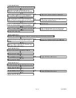
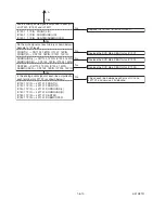
FLOW CHART NO.21
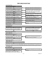
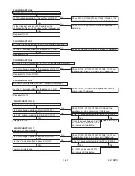
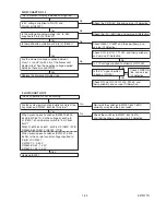
Picture does not appear normally.
Set the disc on the disc tray, and playback.
Are the video signals outputted to each pin of
CN1601 on the AV CBA?
Replace the DVD Main CBA or DVD Mecha.
Check the line between each pin of CN1601 and
each pin of IC6101 on the AV CBA, and service it
if defective.
Is 5V voltage applied to the pin(1, 34) of
IC6101?
Replace IC6101.
Check P-ON+5V line and
service it if defective.
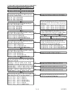
CN1601 1PIN
→
IC6101 6PIN S-Y
CN1601 9PIN
→
IC6101 2PIN S-C
CN1601 7PIN
→
IC6101 16PIN G
CN1601 5PIN
→
IC6101 12PIN B/Cb
CN1601 3PIN
→
IC6101 14PIN R/Cr
Are the video signals shown above inputted into
each pin of IC6101?
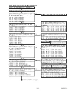
Are the video signals outputted to each pin
of IC6101?
Yes
Yes
No
Yes
Yes
No
No
No
CN1601 1PIN S-Y
CN1601 9PIN S-C
CN1601 7PIN G
CN1601 5PIN B/Cb
CN1601 3PIN R/Cr
IC6101 6PIN S-Y
IC6101 2PIN S-C
IC6101 16PIN G
IC6101 12PIN B/Cb
IC6101 14PIN R/Cr
IC6101 31PIN CVBS
IC6101 28PIN S-Y
IC6101 33PIN S-C
IC6101 19PIN G
IC6101 25PIN B/Cb
IC6101 22PIN R/Cr
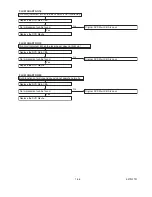
Check the periphery of JK6101 from Pins (19, 22,
25) of IC6101 and service it if defective.
Check the periphery of JK6102 from Pin (22, 25, 28)
of IC6101 and service it if defective.
Check the periphery of JK1401 from
Pin (28) of IC6101 and service it if defective.
Check the periphery of JK1401 from
Pin (33) of IC6101 and service it if defective.
Are the video signals outputted to the specific
output terminal?
Are the component video signals(RGB) outputted
to the VIDEO OUT terminal (JK6101)?
Are the luminance signals outputted to the
S-OUT terminal (JK1401)?
Are the chroma signals outputted to the
S-OUT terminal (JK1401)?
No
No
No
No
No
Are the component video signals(Y/Cb/Cr)
outputted to the VIDEO OUT terminal (JK6102)?
Check the periphery of JK6101 and JK6103 from
Pin(31) of IC6101 and service it if defective.
Are the composite video signals outputted to
the VIDEO OUT terminal (JK6101, JK6103)?
Summary of Contents for DV4400
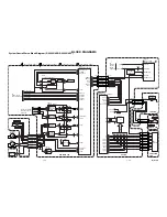
Page 44: ...DVD Main 1 3 Schematic Diagram DV4400 N1B DV4400 N1S 1 8 3 1 8 4 E57M2SCD1 ...
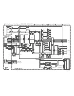
Page 45: ...DVD Main 2 3 Schematic Diagram DV4400 N1B DV4400 N1S 1 8 5 1 8 6 E57M2SCD2 ...
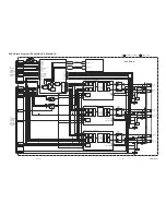
Page 47: ...DVD Main 3 3 Schematic Diagram DV4400 N1B DV4400 N1S 1 8 9 1 8 10 E57M2SCD3 ...
Page 49: ...AV 2 3 Schematic Diagram DV4400 N1B DV4400 N1S 1 8 13 1 8 14 E57M2SCAV2 ...
Page 51: ...DVD Main 1 3 Schematic Diagram DV6400 N1B DV6400 N1S 1 8 17 1 8 18 E57M7SCD1 ...
Page 52: ...DVD Main 2 3 Schematic Diagram DV6400 N1B DV6400 N1S 1 8 19 1 8 20 E57M7SCD2 ...
Page 54: ...1 8 23 1 8 24 E57M7SCD3 DVD Main 3 3 Schematic Diagram DV6400 N1B DV6400 N1S ...
Page 56: ...1 8 27 1 8 28 E57M7SCAV2 AV 2 3 Schematic Diagram DV6400 N1B DV6400 N1S ...
Page 58: ...1 8 31 1 8 32 SACD 1 2 Schematic Diagram DV6400 N1B DV6400 N1S E57M7SCSA1 ...
Page 59: ...1 8 33 1 8 34 SACD 2 2 Schematic Diagram DV6400 N1B DV6400 N1S E57M7SCSA2 ...
Page 64: ...SACD CBA Top View DV6400 N1B DV6400 N1S 1 8 43 BE57D1F02011 1 8 44 ...
Page 65: ...SACD CBA Bottom View DV6400 N1B DV6400 N1S BE57D1F02011 1 8 45 1 8 46 ...
Page 73: ...1 13 3 E57M2EX X10 X2 X4 S2 S2 S4 Unit S1 X13 X1 X5 A22 Packing ...

