DVD Player
DV-18
370K855010 MIT
First Issue 2000.09
Service
Manual
DV18 /
F1N, /K1G, /S1G, /U1G, /U1B
R
D
V
-18
Printed in Japan
Please use this service manual with referring to the user guide ( D.F.U. ) without fail.
TIME
TRACK
TRACK
TITLE
TOTAL
CHAPTER
FTS
SCAN
PBC
TRACK
SVCD
CHAPTER
SHUFFLE
REPEAT
TITLE
A-B
DIGITAL OUT
SURROUND
STANDBY
MAX
PAUSE
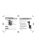
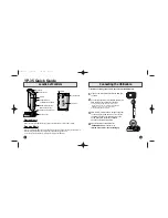
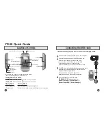
DVD PLAYER DV-18
OPEN/CLOSE
MIN
SHUFFLE
PLAY
DIMMER
SCAN
STOP
POWER
PHONES
LEVEL
V I D E O
TABLE OF CONTENTS
SECTION
PAGE
1. MAIN UNIT
1.1 TECHNICAL SPECIFICATIONS ......................................................................................................... 1-1
1.2 REGIONAL CODES ............................................................................................................................ 1-2
1.3 INFORMATIONS ................................................................................................................................. 1-3
1.4 SERVICING HINT ............................................................................................................................... 1-4
1.5 DISASSEMBLY ................................................................................................................................... 1-5
1.6 REPLACEMENT OF PRINCIPAL COMPONENTS ............................................................................. 1-6
1.7 SERVICE MODE ................................................................................................................................. 1-8
1.8 ELECTRICAL ADJUSTMENT ........................................................................................................... 1-10
1.9 WAVEFORM ..................................................................................................................................... 1-12
1.10 WIRING DIAGRAM ........................................................................................................................... 1-13
1.11 BLOCK DIAGRAM ............................................................................................................................. 1-15
1.12 SCHEMATIC DIAGRAM .................................................................................................................... 1-17
1.13 PARTS LOCATION ........................................................................................................................... 1-27
1.14 EXPLODED VIEW AND PARTS LIST ............................................................................................... 1-30
1.15 ELECTRICAL PARTS LIST ............................................................................................................... 1-33
2. TKM1000MZ ( DVD MODULE for MARANTZ )
2.1 SCHEMATIC DIAGRAM AND PARTS LOCATION ............................................................................. 2-1
2.2 MICROPROCESSOR AND IC DATA ................................................................................................ 2-15
2.3 EXPLODED VIEW AND PARTS LIST ............................................................................................... 2-28
2.4 ELECTRICAL PARTS LIST ............................................................................................................... 2-30
Summary of Contents for dv18
Page 15: ...1 13 1 14 1 10 WARNINGS...
Page 16: ...1 15 1 16 1 11 BLOCK DIAGRAM...
Page 17: ...1 17 1 18 1 12 SCHEMATIC DIAGRAM AND PARTS LOCATION...
Page 18: ...1 19 1 20...
Page 20: ...1 23 1 24...
Page 23: ...1 29 PS01 PK01 QK01 QK04 QK06 QK03 QK05...
Page 34: ...2 1 2 2 Not for DV4000 2 1 SCHEMATIC DIAGRAM AND PARTS LOCATION...
Page 35: ...2 3 2 4...
Page 36: ...2 5 2 6 Not for DV4000...
Page 39: ...2 11 2 12...
Page 45: ...2 20 MN66261 CD signal processing...
Page 46: ...2 21 MN66261 CD signal processing...
Page 47: ...2 22 MN67700 Servo processing IC...
Page 48: ...2 23 MN67700 Servo processing IC...
Page 53: ...2 28 2 3 EXPLODED VIEW AND PARTS LIST TKM1000MZ...