background image


− 

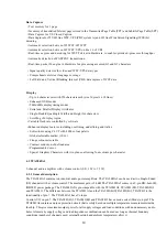
Typical programming time 6ms(< 1 0ms) for up to 16 bytes 

High reliability 

− 

Endurance 106 cycles 1) 

− 

Data retention 40 years 1) 

− 

ESD protection 4000 V on all pins 

8 pin DIP/DSO packages 

Available for extended temperature ranges 

− 

Industrial: - 4 0 t o  

+85 

− 

Automotive: - 4 0 t o  

+125 


4.4.2 Pin Description 

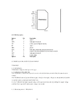
SERIAL CLOCK (SCL): The SCL input is used to positive edge clock data into each EEPROM device and 

negative edge clock data out of each device. 

SERIAL DATA (SDA): The SDA pin is bi-directional for serial data transfer. This pin is open-drain driven 

and may be wire-ORed with any number of other open-drain or open-collector devices. 

The AT24C08 only uses the A2 input for hardwire addressing and a total of two 8K devices may be addressed 

on a single bus system. The A0 and A1 pins are no connects. 

4.4.3 Memory Organization 

T24C16, 16K SERIAL EEPROM: Internally organized with 64 pages of 16 bytes each, the 16K requires a 

10-bit data word address for random word addressing. 

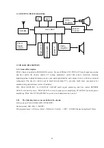
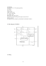
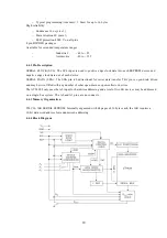
4.4.4 Block Diagram 


18

Summary of Contents for PF21500

Page 1: ...C O L O R T E L E V I S I O N SERVICE MANUAL CHASSISNO ETE 3 Please read this manual carefully before service PF21500 PF21516S MODELNO PF21GB300 李 庆亮 10 11 19 15 05 ...

Page 2: ...ersant with the precautions and procedures for working on high voltage equipment When handling or working on the CRT always discharge the anode to the TV chassis before removing the anode cap in case of electric shock The CRT if broken will violently expel glass fragments Use shatterproof goggles and take extreme care while handling Do not hold the CRT by the neck as this is a very dangerous pract...

Page 3: ...S in this manual during use and servicing of this TV set Otherwise the resulted damage is not protected by the manufacturer 1 4 SAFETY SYMBOL DESCRIPTION The lightning symbol in the triangle tells you that the voltage inside this product may be strong nough to cause an electric shock Extreme caution should be exercised when working on the TV with the back removed This is an international hazard sy...

Page 4: ...utlet and turn on the main power switch of the TV set Operate the TV for at least 15 minutes Degauss the TV set using a specific degaussing coil Set the brightness and contrast to maximum Counter clockwise rotate the R B low brightness potentiometers to the end and rotate the green low brightness potentiometer to center Receive green raster pattern signals Loosen the clamp screw holding the deflec...

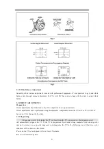
Page 5: ...ned Circumference convergence adjustment Loosen the clamp screw holding the deflection yoke assembly and allow it tilting Temporarily put the first wedge between the picture tube and deflection yoke assembly Move front of the deflection yoke up or down to obtain better convergence in circumference Push the mounted wedge in to fix the yoke temporarily Put the second wedge into bottom Move front of ...

Page 6: ...ents can be performed using the adjustable components inside the TV set For TVs with 2 I C bus control first change the bus data 2 2 1 Degaussing A degaussing coil is built inside the TV set Each time the TV is powered on the degaussing coil will automatically degauss the TV If the TV is magnetized by external strong magnetic field causing color spot on the screen use a specific degausser to demag...

Page 7: ...alue Test Point Voltage 21SS Voltage 21US Voltage Others TP 310V 311 土 5V 311 土 5V 311 土 5V TP 103V 104 土 1 5V 104 土 1 5V 115 土 1 5V TP 184V 184 土 3V 184 土 3V 184 土 3V TP 12V 13 土 1V 16 土 1V 13 土 1V TP 12V 13 土 1V 16 土 1V 13 土 1V TP 22V 22 土 1V 22 土 1V 22 土 1V TP 35V 35 土 1V 35 土 1V 35 土 1V TP 36V 36 土 1V 36 土 1V 36 土 1V TP 5V 1 5 土 0 3V 5 土 0 3V 5 土 0 3V TP 8V 8 土 0 3V 8 土 0 3V 8 土 0 3V TP 5V 2V ...

Page 8: ...d make the horizon accommodation not dazzling white if it doesn t white repeated step until white 7 Regulate to focuse make the light grid focuse good and you get a sharp picture 2 25 SERVICE mode To enter the SERVICE mode Set the volume to 0 Then press and hold the MUTE button on the remote control and press the MENU button on the TV to enter the SERVICE mode To exit from the SERVICE mode turn of...

Page 9: ...OSD VERTICAL SHIFT 50 OSD V6 60Hz OSD VERTICAL SHIFT 46 Fac Factory Bus open 0 Init EEPROM init 0 Page 4 W tone BLOC Common course black level offset 7 BLOR Fine black level offset R 32 BLOG Fine black level offset G 32 BLOB Fine black level offset B 32 WPR White point R 32 WPG White point G 32 WPB White point B 32 Page 5 Tuning IF IF selection 3 TOP 20 AGCS IF AGC SPEED 1 OIF Off set if demodulat...

Page 10: ... stretch 2 XDT X ray detection 0 Page 11 Audio 0 AMLOW Audio output signal for AM sound AM 0 GSSIF Extra gain range SSIF for AM demodulation 0 DSG Gain from audio inputs to audio outputs 0 AGN Gain FM demodulator 0 AGNE Extended gain settings for FM demodulator 1 Page 12 Audio 1 T mod EHT Compensation Set 1 FMWS Window select for FM demodulator 1 BPB2 Bypass sound bandpass filter section 2 1 FFI F...

Page 11: ... and compact circuit with fewer external components The chassis widely used in small and medium TVs provides much more convenience for manufacturing and technical service It includes UOC TDA11136PS N3 3 for PAL NTSC SECAM small signal processing and bus control EEPROM AT24C16 for data memory TDA4864AJ for vertical output power amplifying TFA9842AJ for audio power amplifying Thick film IC FSCQ0765R...

Page 12: ...3 V and they are mounted in an SDIP 64 envelope The features are given in the following feature list 4 1 2 FEATURES TV processor Available in TDA111XX versions Multi standard vision IF circuit with alignment free PLL demodulator Internal switchable time constant for the IF AGC circuit The mono intercarrier sound circuit has a selective FM PLL demodulator which can be switched to the different FM s...

Page 13: ...oupled vertical output stages Horizontal and vertical geometry processing Horizontal and vertical zoom function for 16 9 applications Horizontal parallelogram and bow correction for large screen picture tubes Low power start up of the horizontal drive circuit Macrovision keying possibility for horizontal synchronisation Available in TDA111XX versions A choice can be made between versions with mono...

Page 14: ...underlining and italics Soft colours using CLUT with 4096 colour palette Global selectable matrix 12 16 Fringe colour selectable Contrast reduction of defined area Programmable Cursor Special Graphics Characters with two planes allowing four colours per character 4 2 TFA9842AJ 2 channel audio amplifier with volume control SE 1 W to 7 5 W 4 2 1 General description The TFA9842AJ contains two identic...

Page 15: ...tandby and mute mode No on off switching plops Low standby current High supply voltage ripple rejection Outputs short circuit protected to ground supply and across the load Thermally protected Pin compatible with the TFA9843AJ TFA9843 B J TFA9842 B J TFA9841J 4 2 3 Block diagram of TFA9842AJ 4 2 4 Pining 15 ...

Page 16: ...AGE CIRCUIT TDA4864AJ 4 3 1 FEATURES TDA4864AJ Output current up to 2 5A p p 4 3 2 GENERAL DESCRIPTION The TDA4864AJ is deflection boosters for use in vertical deflection systems for frame frequencies up to 200 Hz The TDA4864AJ needs a separate flyback supply voltage so the supply voltages are independently adjustable to optimize power consumption and flyback time For the TA4864AJ the flyback supp...

Page 17: ...6 bytes Page protection mode flexible page by page hardware write protection Additional protection EEPROM of 64 128 bits bit per data page 1 Protection setting for each data page by writing its protection bit Protection management without switching WP pin Low power CMOS Vcc 2 7 to 5 5V operation Two wire serial interface bus IIC Bus compatible Filtered inputs for noise suppression with Schmitt tri...

Page 18: ...ive edge clock data out of each device SERIAL DATA SDA The SDA pin is bi directional for serial data transfer This pin is open drain driven and may be wire ORed with any number of other open drain or open collector devices The AT24C08 only uses the A2 input for hardwire addressing and a total of two 8K devices may be addressed on a single bus system The A0 and A1 pins are no connects 4 4 3 Memory ...

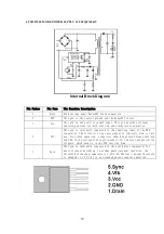
Page 19: ...ly connected to the inverting input of the PWM comparator The collector of an opto coupler is typically tied to this pin For stable operation a capacitor should be placed between this pin and GND If the voltage of this pin reaches 7 5V the over load protection triggers which results in the FPS shutting down 5 Sync This pin is internally connected to the sync detect comparator for quasi resonant sw...

Page 20: ...李 庆亮 10 11 19 15 06 ...
Reviews: