background image

20051207

1-16-1

E6A60EL

ELECTRICAL PARTS LIST

PRODUCT SAFETY NOTE:

 Products marked with a 

#

 have special characteristics important to safety. 

Before replacing any of these components, read 
carefully the product safety notice in this service 
manual. Don't degrade the safety of the product 
through improper servicing.

NOTES: 

1. Parts that are not assigned part numbers (---------) 

are not available.

2. Tolerance of Capacitors and Resistors are noted 

with the following symbols.

Comparison Chart of Models and Marks
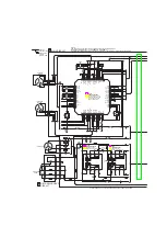
DVD MAIN CBA UNIT

AV CBA

C.....±0.25%

D.....±0.5%

F.....±1%

G.....±2%

J......±5%

K.....±10%

M.....±20%

N.....±30%

Z.....+80/-20%

Model

Mark

MWD200FA A

MWD200FG B

Ref. No. Mark

Description

Part No.

A

DVD MAIN CBA UNIT

N79F0KUP

B

DVD MAIN CBA UNIT

N79F2KUP

Ref. No.

Description

Part No.

AV CBA
Consists of the following:

1VSA12682

CAPACITORS

C1001

#

METALIZED FILM CAP. 0.047

µ

F/ 250V M

CT2E473MS037

C1003

ELECTROLYTIC CAPACITOR 
ZT250TA2R2M6BB

CA2E2R2DYG02

C1004

ELECTROLYTIC CAPACITOR 
ZR200TA820M12BB

CA2D820DYG01

C1005

CERAMIC CAP. B K 120pF/ 500V

CCD2JKP0B121

C1006

#

SAFETY CAP. 2200pF/ 250V

CCD2EMA0E222

C1007

ELECTROLYTIC CAP. 2200

µ

F/ 6.3V

CE0KMASDL222

C1009

ELECTROLYTIC CAP. 1000

µ

F/ 6.3V M

CE0KMASDL102

C1010

CERAMIC CAP.(AX) CH J 560pF/ 50V

CA1J561TU008

C1013

FILM CAP.(P) 0.0033

µ

F/ 50V J

CMA1JJS00332

C1017

CERAMIC CAP.(AX) Y M 0.01

µ

F/ 16V

CCA1CMT0Y103

C1022

CHIP CERAMIC CAP.(1608) B K 0.022

µ

F/ 50V

CHD1JK30B223

C1029

CERAMIC CAP.(AX) X K 2200pF/ 16V

CCA1CKT0X222

C1032

ELECTROLYTIC CAP. 10

µ

F/ 16V M

CE1CMASDL100

C1033

FILM CAP.(P) 0.022

µ

F/ 50V J

CMA1JJS00223

C1034

ELECTROLYTIC CAP. 470

µ

F/ 6.3V M

CE0KMASDL471

C1035

ELECTROLYTIC CAP. 1000

µ

F/ 16V M

CE1CMASDL102

C1037

CHIP CERAMIC CAP.(1608) F Z 0.1

µ

F/ 50V

CHD1JZ30F104

C1038

ELECTROLYTIC CAP. 470

µ

F/ 6.3V M

CE0KMASDL471

C1039

CHIP CERAMIC CAP.(1608) F Z 0.1

µ

F/ 50V

CHD1JZ30F104

C1040

CHIP CERAMIC CAP.(1608) F Z 0.1

µ

F/ 50V

CHD1JZ30F104

C1047

FILM CAP.(P) 0.022

µ

F/ 100V J

CMA2AJS00223

C1048

ELECTROLYTIC CAP. 220

µ

F/ 16V M

CE1CMASDL221

C1201

ELECTROLYTIC CAP. 10

µ

F/ 16V M

CE1CMASDL100

C1202

ELECTROLYTIC CAP. 10

µ

F/ 16V M

CE1CMASDL100

C1207

CHIP CERAMIC CAP.(1608) CH J 68pF/ 50V

CHD1JJ3CH680

C1208

CHIP CERAMIC CAP.(1608) CH J 68pF/ 50V

CHD1JJ3CH680

C1221

ELECTROLYTIC CAP. 10

µ

F/ 16V M

CE1CMASDL100

C1222

ELECTROLYTIC CAP. 10

µ

F/ 16V M

CE1CMASDL100

C1245

CHIP CERAMIC CAP.(1608) F Z 0.1

µ

F/ 50V

CHD1JZ30F104

C1247

ELECTROLYTIC CAP. 470

µ

F/ 6.3V M

CE0KMASDL471

C1249

ELECTROLYTIC CAP. 47

µ

F/ 16V M

CE1CMASDL470

C1351

CHIP CERAMIC CAP.(1608) B K 0.1

µ

F/ 25V

CHD1EK30B104

C1352

ELECTROLYTIC CAP. 47

µ

F/ 6.3V M H7

CE0KMASSL470

C1354

CHIP CERAMIC CAP.(1608) CH J 100pF/ 50V

CHD1JJ3CH101

C1361

CHIP CERAMIC CAP.(1608) F Z 0.1

µ

F/ 50V

CHD1JZ30F104

C1402

ELECTROLYTIC CAP. 470

µ

F/ 6.3V M

CE0KMASDL471

C1403

CHIP CERAMIC CAP.(1608) B K 0.33

µ

F/ 10V

CHD1AK30B334

C1422

CHIP CERAMIC CAP.(1608) B K 0.1

µ

F/ 25V

CHD1EK30B104

C1423

CHIP CERAMIC CAP.(1608) B K 0.01

µ

F/ 50V

CHD1JK30B103

C1443

ELECTROLYTIC CAP. 1000

µ

F/ 6.3V M

CE0KMASDL102

C1524

ELECTROLYTIC CAP. 100

µ

F/ 6.3V M

CE0KMASDL101

C1536

ELECTROLYTIC CAP. 22

µ

F/ 6.3V M H7

CE0KMASSL220

C1537

CHIP CERAMIC CAP.(1608) F Z 0.1

µ

F/ 50V

CHD1JZ30F104

C2031

ELECTROLYTIC CAP. 100

µ

F/ 6.3V M

CE0KMASDL101

C2032

CHIP CERAMIC CAP.(1608) F Z 0.1

µ

F/ 50V

CHD1JZ30F104

C2034

CHIP CERAMIC CAP.(1608) CH J 1000pF/ 50V

CHD1JJ3CH102

CONECTORS

CN1001

22P FFC AV PCB TO MAIN

WX1E5900-001

CN1601

9P FFC AV PCB TO MAIN

WX1E6A60-002

DIODES

D1001

RECTIFIER DIODE 1N4005

NDQZ001N4005

D1002

RECTIFIER DIODE 1N4005

NDQZ001N4005

D1003

ZENER DIODE DZ-22BSBT265

NDTB00DZ22BS

D1004

RECTIFIER DIODE 1N4005

NDQZ001N4005

D1005

RECTIFIER DIODE 1N4005

NDQZ001N4005

D1008

SCHOTTKY BARRIER DIODE SB240-B/P

NDQZ000SB240

D1011

RECTIFIER DIODE BA157

NDQZ000BA157

D1012

SWITCHING DIODE 1N4148M

NDTZ01N4148M

D1015

ZENER DIODE DZ-4.3BSBT265

NDTB0DZ4R3BS

D1018

SWITCHING DIODE 1N4148M

NDTZ01N4148M

D1022

SWITCHING DIODE 1N4148M

NDTZ01N4148M

D1024

SWITCHING DIODE 1N4148M

NDTZ01N4148M

D1025

SWITCHING DIODE 1N4148M

NDTZ01N4148M

D1030

RECTIFIER DIODE FR202-B/P

NDQZ000FR202

D1046

ZENER DIODE DZ-5.6BSCT265

NDTC0DZ5R6BS

D1047

ZENER DIODE DZ-5.1BSBT265

NDTB0DZ5R1BS

D1048

ZENER DIODE DZ-13BSBT265

NDTB00DZ13BS

D1053

PCB JUMPER D0.6-P10.0

JW10.0T

D1054

PCB JUMPER D0.6-P10.0

JW10.0T

D1056

SWITCHING DIODE 1N4148M

NDTZ01N4148M

D1058

SCHOTTKY BARRIER DIODE SB140

NDQZ000SB140

D1059

PCB JUMPER D0.6-P10.0

JW10.0T

D1060

SWITCHING DIODE 1N4148M

NDTZ01N4148M

D1073

PCB JUMPER D0.6-P5.0

JW5.0T

D2010

LED(RED) 204HD/E

NPQZ00204HDE

ICS

IC1001

#

PHOTOCOUPLER PS2561A-1(W)

QPEWPS2561A1

IC1002

VOLTAGE REGULATOR LM1117S-ADJ

NSZBA0T2T001

Ref. No.

Description

Part No.

Summary of Contents for MWD200FG

Page 1: ...SERVICE MANUAL DVD PLAYER MWD200FA MWD200FG OPEN CLOSE PLAY STOP STANDBY ON OPEN CLOSE PLAY STOP IR STANDBY ON ...

Page 2: ...e done or of the possible hazardous consequences of each way Consequently Funai has not undertaken any such broad evaluation Accordingly a servicer who uses a service procedure or tool which is not recommended by Funai must first use all precautions thoroughly so that neither his safety nor the safe operation of the equipment will be jeopardized by the service method selected TABLE OF CONTENTS Spe...

Page 3: ... kΩ load Audio Output 4 Room Ambient 25 C Item Conditions Unit Nominal Limit 1 Video Output 75 Ω load Vpp 1 0 0 1 2 Coaxial Digital Out 75 Ω load mVpp 500 50 3 Audio PCM 3 1 Output Level 1 kHz 0 dB Vrms 1 9 3 2 S N dB 120 3 3 Freq Response DVD fs 48 kHz 20 Hz 22 kHz dB 1 0 CD fs 44 1 kHz 20 Hz 20 kHz dB 1 0 3 4 THD N DVD 1 kHz 0 dB 0 005 CD 1 kHz 0 dB 0 005 ...

Page 4: ...hen the diode is turned on Do not look directly at the laser beam CAUTION Use of controls and adjustments or doing procedures other than those specified herein may result in hazardous radiation exposure Location Top of DVD mechanism Do not look directly at the laser beam coming from the pickup or allow it to strike against your skin Drive Mechanism Assembly Laser Beam Radiation Laser Pickup Turnta...

Page 5: ... especially 1 Wires covered with PVC tubing 2 Double insulated wires 3 High voltage leads D Use specified insulating materials for hazardous live parts Note especially 1 Insulation tape 2 PVC tubing 3 Spacers 4 Insulators for transistors E When replacing AC primary side components transformers power cord etc wrap ends of wires securely about the terminals before soldering F Observe that the wires ...

Page 6: ...ug prongs and externally exposed accessible parts RF terminals antenna terminals video and audio input and output terminals microphone jacks earphone jacks etc is lower than or equal to the specified value in the table below Measuring Method Power ON Insert load Z between B earth ground power cord plug prongs and exposed accessible parts Use an AC voltmeter to measure across the terminals of load ...

Page 7: ...machine then apply hot air to the Flat Pack IC about 5 to 6 seconds Fig S 1 1 2 Remove the flat pack IC with tweezers while applying the hot air 3 Bottom of the flat pack IC is fixed with glue to the CBA when removing entire flat pack IC first apply soldering iron to center of the flat pack IC and heat up Then remove glue will be melted Fig S 1 6 4 Release the flat pack IC from the CBA using tweez...

Page 8: ... by one using a sharp pin or wire to which solder will not adhere iron wire When heating the pins use a fine tip soldering iron or a hot air desoldering machine Fig S 1 4 3 Bottom of the flat pack IC is fixed with glue to the CBA when removing entire flat pack IC first apply soldering iron to center of the flat pack IC and heat up Then remove glue will be melted Fig S 1 6 4 Release the flat pack I...

Page 9: ...rs Fig S 1 6 Note When using a soldering iron care must be taken to ensure that the flat pack IC is not being held by glue When the flat pack IC is removed from the CBA handle it gently because it may be damaged if force is applied 2 Installation 1 Using desoldering braid remove the solder from the foil of each pin of the flat pack IC on the CBA so you can install a replacement flat pack IC more e...

Page 10: ...ed to remove any static electricity that may be charged on the body 2 Ground for Workbench Be sure to place a conductive sheet or copper plate with proper grounding 1 MΩ on the workbench or other surface where the semi conductors are to be placed Because the static electricity charge on clothing will not escape through the body grounding band be careful to avoid contacting semi conductors with you...

Page 11: ... Electrostatic breakdown of the laser diode in the optical system block may occur as a potential difference caused by electrostatic charge accumulated on cloth human body etc during unpacking or repair work To avoid damage of pickup follow next procedures 1 Short the three short lands of FPC cable with solder before removing the FFC cable CN201 from it If you disconnect the FFC cable CN201 the las...

Page 12: ...0DC 2 Front Assembly L 2 L 1 L 1 Fig D2 3 Reinforce Plate S 2 S 2 Fig D3 4 DVD Main CBA Unit S 3 CN201 CN301 CN401 CN601 A Fig D4 View for A Short the three short lands by soldering Either of two places FPC Cable ...

Page 13: ...ghtly into the opening as shown 3 Turn the shaft along with the opening clockwise 4 Repeat steps 2 and 3 until the tray will open 5 Pull the tray slowly manually 5 DVD Mechanism S 4 S 4 S 4 Fig D5 6 AV CBA S 5 L 3 S 6 L 3 Fig D6 B View for B Turn the shaft along with the opening clockwise Rear Front Opening Shaft e g screwdriver ...

Page 14: ...n that order Fig a appears on the screen 2 Press CLEAR button on the remote control unit Fig b appears on the screen When OK appears on the screen the factory default will be set 3 To exit this mode press STANDBY ON button MODEL Version Region EXIT POWER EEPROM CLEAR CLEAR Fig a differ depending on the models MODEL Version Region EEPROM CLEAR OK EXIT POWER EEPROM CLEAR CLEAR differ depending on th...

Page 15: ...ug it again 8 Turn the power on by pressing the STANDBY ON button and the tray will close 9 Press 1 2 3 4 and DISPLAY buttons on the remote control unit in that order Fig g appears on the screen 10 Press CLEAR button on the remote control unit Fig h appears on the screen When OK appears on the screen the factory default will be set Then the firmware renewal mode is complete 11 To exit this mode pr...

Page 16: ...L VREF RESET 70 RESET IC462 1 3 3 3V IC202 OP AMP 15 16 14 13 12 11 17 18 23 6 4 5 3 1 2 25 24 27 26 63 SL AMP 121 SP ROT 3 3V 124 FD OFST 123 TD OFST RESET IC461 2 1 3 3V TO DIGITAL SIGNAL PROCESS BLOCK DIAGRAM DRIVE CBA DVD MAIN CBA UNIT 1 2 6 7 5 3 9 8 10 CN1001 REMOTE SENSOR RM2001 AV CBA 53 POWER 54 OPEN CLOSE 55 STOP 49 REMOTE 56 PLAY CN401 OPEN CLOSE SW2002 POWER SW2003 STOP SW2004 PLAY SW2...

Page 17: ...M INST ROM SERIAL D A GENERAL I O INTERRUPT CONTROLLER TIMER WATCH DOG TIMER REMOTE CONTROL 32BIT CPU STREAM I F EXTERNAL MEMORY I F SDRAM ECC UMAC 100 115 116 113 114 106 104 105 103 62 DEBUG BCU INST CACHE DATA CACHE D A 131 139 Y C VIDEO Y VIDEO C 152 SPDIF 151 AUDIO L MUTE 146 AUDIO R 144 AUDIO L SDRAM ADDRESS 0 10 IC103 FLASH ROM FLASH ROM 29 36 38 45 VIDEO SIGNAL FDQ 0 15 1 9 16 25 48 FADR 0...

Page 18: ...O SIGNAL VIDEO SIGNAL DVD MAIN CBA UNIT AV CBA CN601 8 7 VIDEO Y 10 9 VIDEO C VIDEO Y VIDEO C JK1401 S VIDEO OUT CN1601 Y C TO DIGITAL SIGNAL PROCESS BLOCK DIAGRAM WF1 WF2 WF3 DIGITAL AUDIO OUT COAXIAL 3 3V D2010 POWER JK1402 IC1403 VIDEO DRIVER 4dB AMP 2dB AMP LPF DRIVER 2dB AMP DRIVER 4dB AMP 2dB AMP LPF DRIVER 3 1 5 6 7 VIDEO OUT COMPOSITE SPDIF AUDIO L TO DIGITAL SIGNAL PROCESS BLOCK DIAGRAM A...

Page 19: ... CAUTION Fixed voltage or Auto voltage selectable power supply circuit is used in this unit If Main Fuse F1001 is blown check to see that all components in the power supply circuit are not defective before you connect the AC plug to the AC power supply Otherwise it may cause some components in the power supply circuit to fail NOTE The voltage for parts in hot circuit is measured using hot GND as a...

Page 20: ... in the schematic diagram and the parts list Before replacing any of these components read the parts list in this manual carefully The use of substitute replacement parts that do not have the same safety characteristics as specified in the parts list may create shock fire or other hazards Notes 1 Do not use the part number shown on these drawings for ordering The correct part number is shown in th...

Page 21: ...s were prepared 2 To maintain original function and reliability of repaired units use only original replacement parts which are listed with their part numbers in the parts list section of the service manual 4 Voltage indications for PLAY and STOP mode on the schematics are as shown below 5 How to read converged lines 6 Test Point Information A V F This symbol means fast operating fuse Ce symbole r...

Page 22: ...6A60SCD1 1 NOTE Either IC461 or IC462 is used for DVD MAIN CBA UNIT DVD MAIN 1 3 Ref No Position IC201 C 1 IC202 D 4 IC301 D 3 IC461 F 1 IC462 E 1 Q251 C 2 Q252 B 2 Q253 C 2 Q254 B 2 CN201 A 3 CN301 A 1 CN401 F 3 CONNECTORS ICS TRANSISTORS ...

Page 23: ...1 9 4 DVD Main 2 3 Schematic Diagram E6A60SCD2 ...

Page 24: ...1 9 5 DVD Main 3 3 Schematic Diagram E6A60SCD3 DVD MAIN 3 3 Ref No Position IC103 N 3 IC501 O 4 CN601 R 1 ICS CONNECTOR ...

Page 25: ... NOTE The voltage for parts in hot circuit is measured using hot GND as a common terminal Ce symbole reprèsente un fusible à fusion rapide CAUTION For continued protection against fire hazard replace only with the same type fuse ATTENTION Pour une protection continue les risqes d Incele n utiliser que des fusible de même type Risk of fire replace fuse as marked This symbol means fast operating fus...

Page 26: ...1 9 7 AV 2 2 Schematic Diagram E6A60SCAV2 AV 2 2 Ref No Position IC1201 H 1 IC1403 I 4 Q1201 J 1 Q1202 J 1 Q1204 I 1 Q1351 J 4 CN1601 G 3 ICS TRANSISTORS CONNECTOR ...

Page 27: ...ply Otherwise it may cause some components in the power supply circuit to fail NOTE The voltage for parts in hot circuit is measured using hot GND as a common terminal Ce symbole reprèsente un fusible à fusion rapide CAUTION For continued protection against fire hazard replace only with the same type fuse ATTENTION Pour une protection continue les risqes d Incele n utiliser que des fusible de même...

Page 28: ...it is used in this unit If Main Fuse F1001 is blown check to see that all components in the power supply circuit are not defective before you connect the AC plug to the AC power supply Otherwise it may cause some components in the power supply circuit to fail NOTE The voltage for parts in hot circuit is measured using hot GND as a common terminal Ce symbole reprèsente un fusible à fusion rapide CA...

Page 29: ...01 Pin 7 of CN1601 C1402 PLUS LEAD Pin 11 of CN1601 Pin 13 of CN1601 Pin 9 of CN1601 20µs 0 2V VIDEO Y VIDEO C 0 2V 20µs VIDEO CVBS 0 5V 20µs AUDIO L 0 5V 0 5ms 0 5ms AUDIO R 0 5V 0 5ms SPDIF 1V 0 1µs NOTE Input DVD COLOR BAR SIGNAL WITH 1KHz AUDIO SIGNAL WF1 WF6 ...

Page 30: ...AL AUDIO OUT COAXIAL S VIDEO OUT EV 3 3V 6 3 FS TS DETECTOR 7 9 11 2 3 6 5 M SLED MOTOR M SPINDLE MOTOR 4 AV CBA DVD MAIN CBA UNIT CN1001 is soldered directly to the PCB DRIVE CBA PICK UP UNIT SP 1 SP 2 TRAY IN 6 GND 3 SL 4 SL 5 FS 3 TS 4 GND CD PD 5 GND DVD PD 6 PD MONI 7 DVD LD 8 TS 1 FS 2 GND 11 NU 12 VREF 13 NU 14 B 15 C 16 GND LD 9 CD LD 10 A 17 D 18 CD DVD 19 P ON 5V 20 VIDEO C 10 9 GND 9 8 ...

Page 31: ...L TIMING CHARTS Tray IN TL221 Sled Drive TP303 Disc Drive TP301 Focus Drive TP304 Tracking Drive TP302 0V 3 3V 0V 1 65V 0V 0V 0V 1 65V 1 65V 1 65V Tray Close Play Play Tray Open Tray Close Disc Rotation Play Disc Stop Tray Open ...

Page 32: ... 1 A 2 K 3 E 4 C 8 5 4 1 MM1636XWRE 1 GND 2 Vout 3 Vin E C B E C B Note A Anode K Cathode E Emitter C Collector B Base R Reference G Gate D Drain S Source KIA4558P P KTA1266 Y AT P KTC3203 Y AT P KTA1267 Y AT P KTC3199 GR AT P KTC3199 Y AT P PS2561A 1 W TL432A TA 2SK3498 LM1117S ADJ ...

Page 33: ...1 JK1202 JK1401 JK1402 AV CBA JK1201 See Electrical Parts List for parts with this mark Some Ref Numbers are not in sequence A29 2L041 2L041 2L105 2L021 2L021 DVD MAIN CBA UNIT 2L021 2L011 2L011 1B1 A15 A16 2L031 A1X A22 A23 2L081 2B5 2L081 A21 A A B B ...

Page 34: ...1 14 2 E6A60PEX Packing A22 S1 S2 S4 Unit S2 X10 X5 X2 X4 X1 ...

Page 35: ... A21 A MODEL NO LABEL E6A60UD A21 B MODEL NO LABEL E6AA0UD A22 LABEL BAR CODE E5900UD A23 TELEPHONE NO LABEL H9670UD A29 LABEL EAS L0951UB 1B1 DVD MECHA E7 N79F0KVM N79F0KVM 2B5 REINFORCE PLATE E6A60UD 1VM321919 2L011 SCREW P TIGHT 3X10 BIND HEAD GBHP3100 2L021 SCREW TAP TIGHT M3X11 BIND P TIGHT GBJP3110 2L031 SCREW P TIGHT M3X8 BIND HEAD GBJP3080 2L041 SCREW B TIGHT M3X8 BIND HEAD GBHB3080 2L081 ...

Page 36: ... 16V M CE1CMASDL100 C1222 ELECTROLYTIC CAP 10µF 16V M CE1CMASDL100 C1245 CHIP CERAMIC CAP 1608 F Z 0 1µF 50V CHD1JZ30F104 C1247 ELECTROLYTIC CAP 470µF 6 3V M CE0KMASDL471 C1249 ELECTROLYTIC CAP 47µF 16V M CE1CMASDL470 C1351 CHIP CERAMIC CAP 1608 B K 0 1µF 25V CHD1EK30B104 C1352 ELECTROLYTIC CAP 47µF 6 3V M H7 CE0KMASSL470 C1354 CHIP CERAMIC CAP 1608 CH J 100pF 50V CHD1JJ3CH101 C1361 CHIP CERAMIC C...

Page 37: ...Ω RRXAZR5Z0000 R1077 METAL OXIDE FILM RES 2W J 12 Ω RN02120ZU001 R1080 CHIP RES 1 10W J 2 7k Ω RRXAJR5Z0272 R1081 CHIP RES 1 10W F 220 Ω RRXAFR5H2200 R1086 CHIP RES 1 10W J 3 3k Ω RRXAJR5Z0332 Ref No Description Part No R1091 CHIP RES 1 10W J 47 Ω RRXAJR5Z0470 R1092 PCB JUMPER D0 6 P5 0 JW5 0T R1093 CHIP RES 1 10W J 470 Ω RRXAJR5Z0471 R1205 CHIP RES 1 10W F 11k Ω RRXAFR5H1102 R1206 CHIP RES 1 10W ...

Page 38: ...MWD200FA MWD200FG E6A60 A0UD 2005 12 27 ...

Reviews: