background image

6-4

Specifications

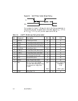
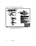
Figure 6.3

L64777 Bus 3-state Delay Timing

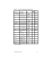
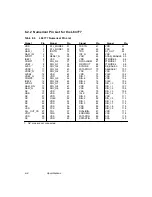
The numbers in column 1 of Table 6.4 refer to the timing parameters in
the preceding figures. All parameters in this table apply for T

A

= 0

°

C to

85

°

C, V

DD

= 3.1 V to 3.6 V, and an output load of 50 pF.

TN

DATA

11

11

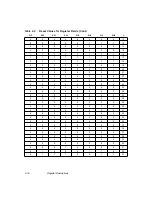
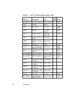
Table 6.4

L64777 Preliminary Timing Parameters

No.

Parameter

Description

Min

Max

Unit

1

tCYCLE

Clock Cycle OCLK

32

ns

2

tPWH

Clock Pulse Width HIGH OCLK

7

ns

3

tPWL

Clock Pulse Width LOW OCLK

7

ns

4

tI_CYCLE

Clock Cycle ICLK

18.5

ns

5

tI_PWH

Clock Pulse Width HIGH ICLK

9

ns

6

tI_PWL

Clock Pulse Width LOW ICLK

9

ns

7

tI_S

Input Setup Time to ICLK

6

ns

8

tI_H

Input Hold to ICLK

2

ns

9

tRWH

Reset Pulse Width HIGH

50

ns

10

tWK

Wake-up Time after RESET
(used for RAM initialization during
microprocessor configuration
access)

1280

2560

ICLK cycles with

DVALIDIN =

HIGH

OCLK cycles

11

tTDLY

Delay from TN

20

ns

Summary of Contents for L64777

Page 1: ...L64777 DVB QAM Modulator Order Number I14031 A Technical Manual June 2000...

Page 2: ...ation reserves the right to make changes to any products herein at any time without notice LSI Logic does not assume any responsibility or liability arising out of the application or use of any produc...

Page 3: ...benefit from this book are Engineers and managers who are evaluating the modulator for possible use in a system Engineers who are designing the modulator into a system Organization This document has t...

Page 4: ...e internal signals Related Publications Digital Broadcasting Systems for Television Sound and Data Services Framing Structure Channel Coding and Modulation Cable Systems ETS 300 429 September 1996 Gen...

Page 5: ...Input Synchronization 2 10 2 4 1 Sync Acquisition Phase 2 13 2 4 2 Sync Tracking Phase 2 14 2 5 FIFO Clock Conversion 2 16 2 6 Sync EF Reinsertion Unit 2 17 2 6 1 Sync Insertion Mode 2 18 2 6 2 Error...

Page 6: ...3 Interfaces 3 1 Transport Interface 3 1 3 1 1 Synchronization 3 1 3 1 2 Synchronization Methods 3 2 3 1 3 Transport Error Indicator Handling 3 2 3 2 Serial Control Interface 3 2 3 3 Analog Output Int...

Page 7: ...2 17 Register 42 4 17 4 2 18 Register 43 4 17 Chapter 5 Signals 5 1 Overview 5 1 5 2 MPEG Transport Stream Multiplexer Signals 5 3 5 3 Status Information Signals 5 4 5 4 Test Signals 5 5 5 5 Control S...

Page 8: ...ice Internal Signals Customer Feedback Figures 1 1 L64777 Operating Environment 1 2 2 1 ETS 300 429 Compliant Modulation Operation 2 2 2 2 Data Path 2 3 2 3 Phase and Frequency Detection with an Exter...

Page 9: ...PE Mechanical Drawing 6 11 A 1 Quick Overview of the Serial Bus A 2 A 2 Serial Bus Write Read Cycle A 3 A 3 General Call Structure A 4 A 4 Burst Write to Slave Master Transmitter Slave Receiver A 5 A...

Page 10: ...x Contents...

Page 11: ...ons digital to analog converters and sampling clock circuitry that generates a quadrature amplitude modulation QAM modulated output signal in baseband Users can configure the device by means of its se...

Page 12: ...nt modulation operation Highly integrated global synchronization and clock control On chip VCO to support symbol rates up to 10 Msymbols s Digital NCO and interpolation mode to support operation with...

Page 13: ...buffer IEEE 1149 1 JTAG interface for testing Up to 10 Mbytes s parallel data input Up to 60 Mbits s serial data input Up to 11 25 Mbaud operation in NCO mode of operation Easy interface to most inpu...

Page 14: ...1 4 Introduction...

Page 15: ...Input Synchronization page 2 10 Section 2 5 FIFO Clock Conversion page 2 16 Section 2 6 Sync EF Reinsertion Unit page 2 17 Section 2 7 Reed Solomon Encoder page 2 20 Section 2 8 Convolutional Interlea...

Page 16: ...nchronizing stage The OCLK which is four times the QAM symbol rate is the base of all residual processing A numerically controlled oscillator NCO module allows the L64777 to interface with LSI Logic L...

Page 17: ...icroprocessor Interface OCLK 1 Data Square Root Nyquist Filter Circular I Q Diff Encoder Input Sync Energy Dispersal 8 SCAN chain JTAG Test RAMbist Sync FIFO Error flag Reinsertion Stage Buffer Symbol...

Page 18: ...cept an external VCO Mode 2 connects the PCLK output of L64724 or L64734 to the L64777 PCLK clock input and connects the byte clock output to the ICLK input of the L64777 This is also called the Numer...

Page 19: ...Consecutive sync blocks can have any gap length between them Thus the L64777 can convert an input block to a block with a gap for RS insertion as long as the size of the 128 byte circular input buffer...

Page 20: ..._INDICATOR bit of MPEG transport packets Either the FSTARTIN pulse or the SYNC_BYTE detection 0x47 for MPEG transport packets establishes input synchronization The FSTARTIN pulse marks the first bit t...

Page 21: ...t format can be programmed either as a two s complement or as a sign magnitude representation The analog I and Q modulated output signals are at a sampling rate of OCLK which is four times the QAM sym...

Page 22: ...FIRSTOUT indicates the head of a sequence after reset with the SSTARTIN signal The negative slope of the SSTARTIN input pin controls sequence reset Note DVALIDIN must be active for at least one ICLK...

Page 23: ...l interface can transfer reads and writes in single byte or burst mode It must access the status registers 12 and 13 with single byte reads The division factor for converting OCLK down to the symbol c...

Page 24: ...bytes and strips off invalid data The transport interface can operate in either Parallel or Serial mode The L64777 can synchronize the transport interface in two ways In both modes it works synchrono...

Page 25: ...sync stage issues the control strobes for the downstream modules In addition to synchronizing the L64777 to SYNC_BYTEs contained in the input stream the L64777 can be forced into synchronization by e...

Page 26: ...all generated sequences run free When using the L64777 with the L64724 select Parallel mode which is supported with external synchronization pulses Use the SPI of L64724 in Mode 2 204 cycle frames wit...

Page 27: ...select from three values of track steps which are the number of flywheel repetitions required to declare the states SYNCOK and loss of sync There are two phases to the sync algorithm procedure the sy...

Page 28: ...Phase The sync tracking phase checks the detection of S at the correct location i e every P bytes TS 1 mismatches are tolerated but at the last mismatch the L64777 declares a loss of sync and goes bac...

Page 29: ...tion test This transition activates a declaration of loss of sync The L64777 activates output SYNCOK in state S3 S4 or S5 This allows easy measurement of synchronization conditions from outside and mo...

Page 30: ...frequency relationship determines how the read and write pointers advance To allow outside watching of the asynchronous pointers an alarm comparator indicates when both pointers are equal Because bot...

Page 31: ...very time the L64777 accesses the FIFO delay value in the microprocessor interface FDEL see Section 4 1 3 Register 2 page 4 5 the pointers are reset to the these values If the L64777 is programmed to...

Page 32: ...ocessing task is the error flag handling for MPEG 2 transport packets If ERRORIN indicates a decoder error at the first byte of a frame the L64777 sets the TRANSPORT_ERROR_INDICATOR bit of the MPEG 2...

Page 33: ...7 uses a special sync word 0xB8 generated by inverting every eighth transport sync word 0x47 to align the descrambler with the incoming data stream The L64777 applies the first bit of the PRBS to the...

Page 34: ...d length N and the second indicating the number of message bytes K The difference between these two numbers N K is the number of check bytes DVB uses this generator polynomial for RS codes where R 16...

Page 35: ...e bytes and the number of check bytes K R t Number of Error Corrections This variable is the maximum number of error corrections performed by the decoder Its maximum value is 2 7 1 Forward Error Corre...

Page 36: ...struct the original message precisely from the check symbols as long as the code word has no more than byte errors where R the number of redundant check bytes 2 7 2 Error Handling and Correction A bit...

Page 37: ...t The scheme is also referred to as a convolutional interleaver deinterleaver based on the Forney approach Figure 2 15 Interleaver Block Diagram The L64777 interleaver performs periodic interleaving w...

Page 38: ...this value which is 1122 valid clock cycles If the QAM is not in 256 mode the interleaver inserts invalid cycles in an eight byte sequence which proportionally increases the delay time The zero delay...

Page 39: ...b2 b1 b0 Symbol t Symbol t Symbol t 1 Symbol t 1 Symbol t 2 Symbol t 3 Symbol t 2 Symbol t 3 Symbol t 4 Symbol t 5 b5 b4 b3 b2 b1 b0 b5 b4 b3 b2 b1 b0 b5 b4 b3 b2 b1 b0 m 8 m 4 m 6 Time Byte 4 Byte 0...

Page 40: ...he underlying concepts in Figure 2 18 here are two examples 1 If m 4 Ak is bit 3 Bk is bit 2 and the LSB m 2 bits bits 1 0 2 If m 6 Ak is bit 5 Bk is bit 4 and the LSB m 2 bits bits 3 0 Equation 2 1 E...

Page 41: ...l is a result of the length of each coefficient register 211 plus the length of INQ 24 plus the number of stages 30 25 The total number of coefficients is 124 there is one coefficient set for each of...

Page 42: ...coefficients except that it adds them directly to the MAC outputs There is one offset coefficient for each phase The shifter block adjusts the internally generated filter result to accommodate the li...

Page 43: ...nterpolator for example to 3 rather than 5 2 11 1 Filter Setup Procedure The filter module is loaded with 31 filter coefficients sequentially with four blocks of 49 bytes in the PHASE_0 PHASE_1 PHASE_...

Page 44: ...6 write cycles the four coefficient register banks are completely configured During configuration the filter is not operational to save gates by avoiding double buffering of the coefficient registers...

Page 45: ...8 c13 10 c13 9 c13 8 20 c14 7 c14 6 c14 5 c14 4 c14 3 c14 2 c14 1 c14 0 21 c15 7 c15 6 c15 5 c15 4 c15 3 c15 2 c15 1 c15 0 22 c14 10 c14 9 c14 8 c15 10 c15 9 c15 8 23 c16 7 c16 6 c16 5 c16 4 c16 3 c1...

Page 46: ...27 8 41 c28 7 c28 6 c28 5 c28 4 c28 3 c28 2 c28 1 c28 0 42 c29 7 c29 6 c29 5 c29 4 c29 3 c29 2 c29 1 c29 0 43 c28 10 c28 9 c28 8 c29 10 c29 9 c29 8 44 c30 7 c30 6 c30 5 c30 4 c30 3 c30 2 c30 1 c30 0 4...

Page 47: ...28 95 14 191 184 29 257 15 593 862 965 862 16 593 257 29 184 17 191 95 28 105 18 107 48 26 71 19 69 27 23 51 20 46 15 20 38 21 31 8 16 28 22 20 3 13 19 23 14 1 10 13 24 8 1 7 9 25 4 1 5 5 26 3 1 3 3 2...

Page 48: ...control generates the clocking for the input and output interfaces it also controls the data path It contains all the necessary logic to chain the processing units together 0 0 1 0 2 0 3 0 4 0 5 0 6 0...

Page 49: ...OCLK divider 32 ICLK divider 6 for 64 QAM 2 12 1 Numerically Controlled Oscillator NCO In PLL Mode 2 an NCO generates the internal clocking OCLK SCLK and the control information for the interpolator T...

Page 50: ...er 14 page 4 12 can control the start of the measurement and the Measurement Done bit in register 13 indicates successful completion If bit 2 of Register 14 enables an interrupt the measurement genera...

Page 51: ...example 188 ld QAMmode is the number of bits per QAM symbol If the RS encoder is enabled in DVB mode and the SPI interface of L64724 is programmed to Mode 2 the factor of sync length by valid bytes b...

Page 52: ...to 18 measurement duration ref dur Registers 21 22 threshold reg 43 reset virtual FIFO step step virtual FIFO nco_gain wait until measurement duration has elapsed reset virtual FIFO abs virt FIFO thre...

Page 53: ...the ENABLE_PHASE_LOOP bit is set in the NCO control register Register 14 bit 1 the loop starts running a phase compare between the divided reference and the divided feedback clock The NCO must set co...

Page 54: ...r FIFO initialization The microprocessor interface uses an I2 C compatible serial control protocol The signal behavior is described in Appendix A The interface is slave only and can not be a master to...

Page 55: ...of SSTARTIN to reset all sequences at the beginning of the next sync block Apply a negative slope of SSTARTIN after all mode changes from the microprocessor interface and wait for FIRSTOUT Also the s...

Page 56: ...rinted circuit board environment an additional IEEE 1149 1 JTAG module is included in the device which operates on the following pins TRSTn 0 TCK 0 TMS 0 TDI 0 TDO output Special test modes are applic...

Page 57: ...ation bytes and to strip off invalid data The transport interface can operate in either parallel or serial mode 3 1 1 Synchronization The L64777 can synchronize the transport interface in two ways In...

Page 58: ...rt interface can program the block length and the value of the sync byte The block length must be less than 256 bytes After the L64777 achieves synchronization it inserts the sync byte into the modula...

Page 59: ...s to load the filter coefficients it does not apply an autoincrement to APR0 If APR0 is not at zero the Serial Control Interface expects only a single data byte and applies an autoincrement to the APR...

Page 60: ...h the outputs of the two L64777 DACs AVDD1 COMP1 Vref1 10 Bit DAC 10 AVSS2 AVDD2COMP2 Differential Q Output Differential I Output VSS AVSS1 R VDDX1 3 On Chip Off Chip QAM_I QAM_In QAM_Q QAM_Qn Q Filte...

Page 61: ...R17 221 1 2 3 4 NC IN IN VS NC VS OUT NC 8 7 6 5 F TH4 TH 1 R18 51 AD8048AR F R19 51 F R20 51 F R21 511 F C35 10 F 16 V C34 0 1 5 V A 5 V A F C42 10 F 16 V C43 0 1 TH8 TH TH7 TH QAM_Q QAM_QN 1 1 R35 2...

Page 62: ...e termination to both differential lines and the DAC achieves maximum linearity in differential mode 3 4 Digital Output Interface The L64777 I and Q component outputs are available in 10 bit digital f...

Page 63: ...er coefficient register A0 is a sequential input register which sequentially shifts in the 196 bytes of filter coefficients Therefore the external microprocessor must make exactly 196 accesses to that...

Page 64: ...ICNT_I 3 ICNT_I 2 ICNT_I 1 ICNT_I 0 R W 9 RESERVED I_ICNT_I 14 ICNT_I 13 ICNT_I 12 ICNT_I 11 ICNT_I 10 ICNT_I 9 ICNT_I 8 R W 10 TRACK STEPS 1 TRACK STEPS 0 UNCON STR INPUT GAP 4 GAP 3 GAP 2 GAP 1 GAP...

Page 65: ...OUNT 16 R 31 NP_COUNT 7 NP_COUNT 6 NP_COUNT 5 NP_COUNT 4 NP_COUNT 3 NP_COUNT 2 NP_COUNT 1 NP_COUNT 0 R 32 NP_COUNT 15 NP_COUNT 14 NP_COUNT 13 NP_COUNT 12 NP_COUNT 11 NP_COUNT 10 NP_COUNT 9 NP_COUNT 8...

Page 66: ...Insertion R W 6 When this bit is 1 the L64777 inserts a new sync word NEWSYNC see Section 2 6 1 into the data stream When this bit is 0 the L64777 leaves the data stream unchanged The reset value is...

Page 67: ...ocation loads the ICLK address counter with 0 and the OCLK driven address counter to the FDEL value If the FIFO is automatically reset the L64777 also uses this value for the OCLK driven address The r...

Page 68: ...module by two clock cycles When this bit is 0 the L64777 runs the RS encoder normally The reset value is 0 INT_OFF Interleaver Off R W 1 When this bit is 1 the L64777 stops the interleaver and delays...

Page 69: ...am The interleaver RAM resumes normal operation as soon as the first sequence start from the SSTARTIN pin pin 90 comes in the data stream This setting is useful for getting a well defined chip output...

Page 70: ...h power mode with lower jitter For normal operation set this bit to 0 RES Reserved 0 This bit is reserved 4 1 8 Registers 7 and 8 RES Reserved 15 This bit is reserved ICNT_O Initial OCLK Value R W 14...

Page 71: ...eset value is 0 GAP RS Code Bytes R W 4 0 This is the number of bytes to be inserted for the RS code at each end of a sync block If the value is 0 there is no modification of the incoming data stream...

Page 72: ...is set to 1 if a FIFO alarm condition is detected since the last read If this bit is 0 no FIFO alarm condition was detected The reset value is 0 ERF_STORE Error Flag Store R 4 This read only bit is se...

Page 73: ...0 MEASUREMENT_DONE R 5 A 1 in this bit indicates that the measurement data gained during byte clock probe are valid and that the measurement is complete The reset value is 0 STEP_UPDATE R 4 A 1 in thi...

Page 74: ...pt the status is indicated correctly The reset value is 0 AUTO_ACQUISITION_ON R W 3 A 1 to 0 transition in this bit starts an internal procedure to regulate the NCO frequency The reset value is 0 Sett...

Page 75: ...NCO step parameter It is loaded into the NCO when the most significant portion is written These are NCO related register fields they are used only in PLL Mode Bits 8 and 23 are reset to 0 all other bi...

Page 76: ...measurement in units of 256 ICLK cycles These are NCO related register fields they are used only in PLL Mode 2 The reset value is 0 4 2 9 Register 25 N_PCLK PCLK Cycles R W 7 0 R This is the number o...

Page 77: ...PLL Mode 2 The reset value is 0 4 2 12 Registers 32 33 and 34 NP_COUNT R 23 0 This value is the number of ICLK cycles found within the duration of n 1 PCLK cycles The value in this register is valid...

Page 78: ...4 2 15 Register 40 FIFO_FULL FIFO Fullness Indicator R 7 0 This value is a sign representation of the virtual FIFO fullness used for the NCO loop regulation These are NCO related register fields they...

Page 79: ...measurement which is used as the initial value for the autoacquisition These are NCO related register fields they are used only in PLL Mode 2 The reset value is 0b0111 0011 Table 4 2 shows the reset v...

Page 80: ...0 0 0 0 24 0 0 0 0 0 0 0 0 25 0 0 0 0 0 0 0 0 26 0 0 0 0 0 0 0 0 27 0 0 0 0 0 0 0 0 28 0 0 0 0 0 0 0 0 29 0 0 0 0 0 0 0 0 30 0 0 0 0 0 0 0 0 31 0 0 0 0 0 0 0 0 32 0 0 0 0 0 0 0 0 33 0 0 0 0 0 0 0 0 3...

Page 81: ...3 Section 5 3 Status Information Signals page 5 4 Section 5 4 Test Signals page 5 5 Section 5 5 Control Signals page 5 6 Section 5 6 External PLL Signals page 5 6 Section 5 7 Analog QAM Signals page 5...

Page 82: ...g DIN 7 0 L64777 QAM Modulator ICLK FSTARTOUT PLL_OUT_CS SSTARTIN TESTPINS 11 0 SYNCOK FSTARTIN FIFOALARM QAM_Q PLL_MODE 1 0 SCL SDA SB_BASE 1 0 AVSS1 AVDD1 COMP1 AVSS2 AVDD2 COMP2 VREF_I IREF1 IREF2...

Page 83: ...IN pin is asserted to flag uncorrectable errors The L64777 checks the ERRORIN status at the first bit of a frame then if required HIGH set error bit it copies the value of that bit to the MPEG error i...

Page 84: ...s Information Signals DIG_I 9 0 Digital I Component Output This port provides modulator I component output in digital format Depending on the PLL mode either OCLK or PCLK is the related clock DIG_Q 9...

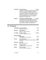
Page 85: ...onization status when HIGH This signal is asserted when the number of track steps required for synchronization is fulfilled If FSTARTIN pulses force synchronization SYNCOK is constantly LOW 5 4 Test S...

Page 86: ...in resets all internal data paths Reset timing is asynchronous to the device clocks Reset affects all the configuration registers and the filter coefficients which must be downloaded again after reset...

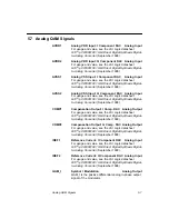
Page 87: ...Digital Synthesis Digital to Analog Converter September 1998 COMP1 Compensation Output I Comp DAC Analog Output For usage and value see the LSI Logic datasheet G10 p CW900100 10 bit Direct Digital Sy...

Page 88: ...to Analalog Converter Q Channel For usage and value see the LSI Logic datasheet G10 p CW900100 10 bit Direct Digital Synthesis Digital to Analog Converter September 1998 VREF_I Reference Voltage Inpu...

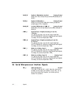
Page 89: ...evice because they determine the two LSBs of the serial bus base address SCL Serial Clock Line Input In conjunction with SDA SCL controls the microprocessor interface according to the protocol describ...

Page 90: ...5 10 Signals...

Page 91: ...nout page 6 10 6 1 AC DC Specifications This section lists the electrical requirements provides the AC timing characteristics shows the AC timing diagrams and lists the AC timing values for the L64777...

Page 92: ...Temperature Range Plastic 40 to 150 C TJ Operating Junction Temperature Range 0 to 125 C Table 6 2 L64777 Recommended Operating Conditions Symbol Parameter Limits Unit VDD DC Supply 3 14 to 3 45 V TA...

Page 93: ...ge VDD Max VIN VDD or VSS 10 1 10 mA IIN Input Current Leakage w Pullup VDD Max VIN VDD or VSS 62 215 384 mA IIN Input Current Leakage w Pulldown VDD Max VIN VDD or VSS 62 215 384 mA IDD Quiescent Sup...

Page 94: ...tion Min Max Unit 1 tCYCLE Clock Cycle OCLK 32 ns 2 tPWH Clock Pulse Width HIGH OCLK 7 ns 3 tPWL Clock Pulse Width LOW OCLK 7 ns 4 tI_CYCLE Clock Cycle ICLK 18 5 ns 5 tI_PWH Clock Pulse Width HIGH ICL...

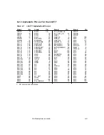
Page 95: ...y Mnemonic Description Type Drive mA Active AVDD1 Supply for DAC Analog Input AVDD2 Supply for DAC Analog Input AVSS1 Analog Supply for DAC Analog Input AVSS2 Supply for DAC Analog Input COMP1 Compens...

Page 96: ...put Bidirectional LOW HIGH PCLK Clock Input for PLL Mode 2 TTL input HIGH PLL_MODE 1 0 Select PLL Mode Input w Pulldown HIGH PLL_OUT_CS PLL Current Source 3 state Current Source 4 3 state QAM_I Positi...

Page 97: ...G Test Clock TTL Input w Pulldown 1 TDI JTAG Test Data In TTL Input w Pulldown HIGH TDO JTAG Test Data Out Output 4 HIGH TMS JTAG Test Mode Select TTL Input w Pulldown HIGH TNn 3 State Mode TTL Input...

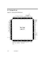
Page 98: ...EF_Q 13 COMP2 14 IREF2 15 AVDD2 16 QAM_QN 17 QAM_Q 18 NC 19 GND 20 NC 21 NC 22 NC 23 NC 24 NC 25 VSS 26 PLL_OUT_CS 27 VDD 28 VDD 29 NC 30 PLL_MODE 0 31 PLL_MODE 1 32 IDDTN 33 TN 34 RESET_N 35 VSS 36 D...

Page 99: ...37 DIG_Q 1 38 DIG_Q 2 39 DIG_Q 3 40 DIG_Q 4 41 DIG_Q 5 44 DIG_Q 6 45 DIG_Q 7 46 DIG_Q 8 47 DIG_Q 9 48 DIN 0 84 DIN 1 83 DIN 2 82 DIN 3 81 DIN 4 76 DIN 5 75 DIN 6 74 DIN 7 73 DVALIDIN 87 ERRORIN 88 FIF...

Page 100: ...SS VSS DIG_Q 9 DIG_Q 8 DIG_Q 7 DIG_Q 6 DIG_Q 5 VDD VSS DIG_Q 4 DIG_Q 3 DIG_Q 2 DIG_Q 1 DIG_Q 0 VSS RESET_N TN IDDTN PLL_MODE 1 PLL_MODE 0 SSTARTIN FSTARTIN ERRORIN DVALIDIN VDD VSS DIN 0 DIN 1 DIN 2 D...

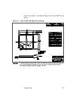
Page 101: ...he L64777 Figure 6 5 120 Pin PQFP PE Mechanical Drawing Important This drawing may not be the latest version For board layout and manufacturing obtain the most recent engineering drawings from your LS...

Page 102: ...anical Drawing Cont Important This drawing may not be the latest version For board layout and manufacturing obtain the most recent engineering drawings from your LSI Logic marketing representative by...

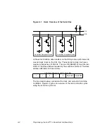
Page 103: ...Section A 2 Programming the Slave Address Using the Serial Bus Interface page A 4 shows how the slave address is formed and transmitted Section A 3 Write Cycle Using the Serial Bus Interface page A 4...

Page 104: ...cy of 400 kHz The pins SB_BASE 1 0 input the two LSB s of the slave address required by the serial bus protocol The slave address definition is shown below The bus master always generates the clock an...

Page 105: ...nsmitter Slave Receiver ACK Cycle Slave Master Receiver Slave Transmitter Single Read Cycle bit7 bit6 bit5 bit3 bit2 bit1 bit0 bit4 bit7 bit6 bit5 bit4 bit3 bit2 bit1 Master transmits slave address Sl...

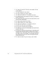
Page 106: ...cle Using the Serial Bus Interface Figure A 4 shows the timing for a burst or a single write cycle The following cycles must take place for a write cycle 1 The master starts the cycle with the start c...

Page 107: ...by issuing a start condition 2 The master transmits the 7 bit slave address 3 The master sets the R W bit 0 to indicate a write cycle 4 The addressed slave acknowledges the reception of the slave addr...

Page 108: ...ndition 13 The master transmits the 7 bit slave address 14 The master sets the R W bit 1 to indicate a read cycle 15 The slave drives SDA LOW to acknowledge 16 The slave starts transmitting the data M...

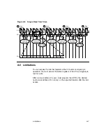
Page 109: ...desired next access address Do not rely on the expected location after the last access Start Stop SCL SDA Condition Condition Bit 7 Bit 6 Bit 5 Bit 7 Bit 6 Bit 5 Bit 4 Bit 3 Bit 2 Bit 1 R W ACK Slave...

Page 110: ...A 8 Programming the L64777 in Serial Host Interface Mode...

Page 111: ...B 1 Section B 2 PLL Driver Settings for Typical Applications page B 2 Section B 3 Connecting the L64777 to the LSI Logic L64724 page B 3 B 1 Overview The QAM modulator is the last stage in a digital C...

Page 112: ...ce or the L64724 satellite receiver The relationship among the SCLK OCLK and input data rate is described in the following subsections If the same serial host controls both the L64724 and the L64777 h...

Page 113: ...terfacing the L64724 supports two modes of byte clock generation Mode 2 of the synchronous parallel interface SPI is best suited for interconnection with L64777 In this mode the L64724 outputs 204 byt...

Page 114: ...l Mode NCO mode Mode 2 Block Length 188 bytes GAP 16 bytes I Counter 6 0x6 O Counter 32 0x20 After synchronization OCLK Baud rate x 2 x 3 4 x oversampling x 1 symbol size SCLK OCLK 4 where oversamplin...

Page 115: ...IFO output 0b0010 Scrambler output 0b0011 RS encoder output 0b0100 Interleaver output 0b0101 M tuple output 0b0110 Mapper output 0b0111 N A 0b1000 Interpolator control 0b1001 NCO step bit 23 16 on DIG...

Page 116: ...C 2 Monitoring Device Internal Signals...

Page 117: ...o us at the number shown If appropriate please also fax copies of any marked up pages from this document Important Please include your name phone number fax number and company address so that we may c...

Page 118: ...f appropriate please fax a marked up copy of the page s Please complete the information below so that we may contact you directly for clarification or additional information Excellent Good Average Fai...

Page 119: ...727 507 5000 Georgia Atlanta A E Tel 770 623 4400 B M Tel 770 980 4922 W E Tel 800 876 9953 Duluth I E Tel 678 584 0812 Hawaii A E Tel 800 851 2282 Idaho A E Tel 801 365 3800 W E Tel 801 974 9953 Ill...

Page 120: ...781 271 9953 South Carolina A E Tel 919 872 0712 W E Tel 919 469 1502 South Dakota A E Tel 800 829 0116 W E Tel 612 853 2280 Tennessee W E Tel 256 830 1119 East West A E Tel 800 241 8182 Tel 800 633...

Page 121: ...ton Mint Technology 77 South Bedford Street Burlington MA 01803 Tel 781 685 3800 Fax 781 685 3801 Minnesota Minneapolis 8300 Norman Center Drive Suite 730 Minneapolis MN 55437 Tel 612 921 8300 Fax 612...

Page 122: ...Singapore Singapore LSI Logic Pte Ltd 7 Temasek Boulevard 28 02 Suntec Tower One Singapore 038987 Tel 65 334 9061 Fax 65 334 4749 Sweden Stockholm LSI Logic AB Finlandsgatan 14 164 74 Kista Tel 46 8...

Page 123: ...ei Time24 Bldg 35 Tansu cho Shinjuku ku Tokyo 162 0833 Tel 81 3 3260 1411 Fax 81 3 3260 7100 Technical Center Tel 81 471 43 8200 Marubeni Solutions 1 26 20 Higashi Shibuya ku Tokyo 150 0001 Tel 81 3 5...

Page 124: ......
Reviews: