


LT3956
3956f
applicaTions inForMaTion
20mV should not cause misoperation, but may lead to
noticeable offset between the average value and the user-
programmed value.
Output Current Capability
An important consideration when using a switch with a
fixed current limit is whether the regulator will be able
to supply the load at the extremes of input and output
voltage range. Several equations are provided to help
determine this capability. Some margin to data sheet
limits is included.
For boost converters:
I
A
V
V
OUT MAX
IN MIN
OUT MAX
(
)
(
)
(
)
.
≤
2 5
For buck mode converters:
I
OUT(MAX)
≤
2.5A
For SEPIC and buck-boost mode converters:
I
A
V
V
V
OUT MAX
IN MIN
OUT MAX
IN MIN
(
)
(
)
(
)
(
)
.
(
)
≤
+
2 5
These equations assume the inductor value and switch-
ing frequency have been selected so that inductor ripple
current is ~600mA. Ripple current higher than this value
will reduce available output current. Be aware that current
limited operation at high duty cycle can greatly increase
inductor ripple current, so additional margin may be
required at high duty cycle.
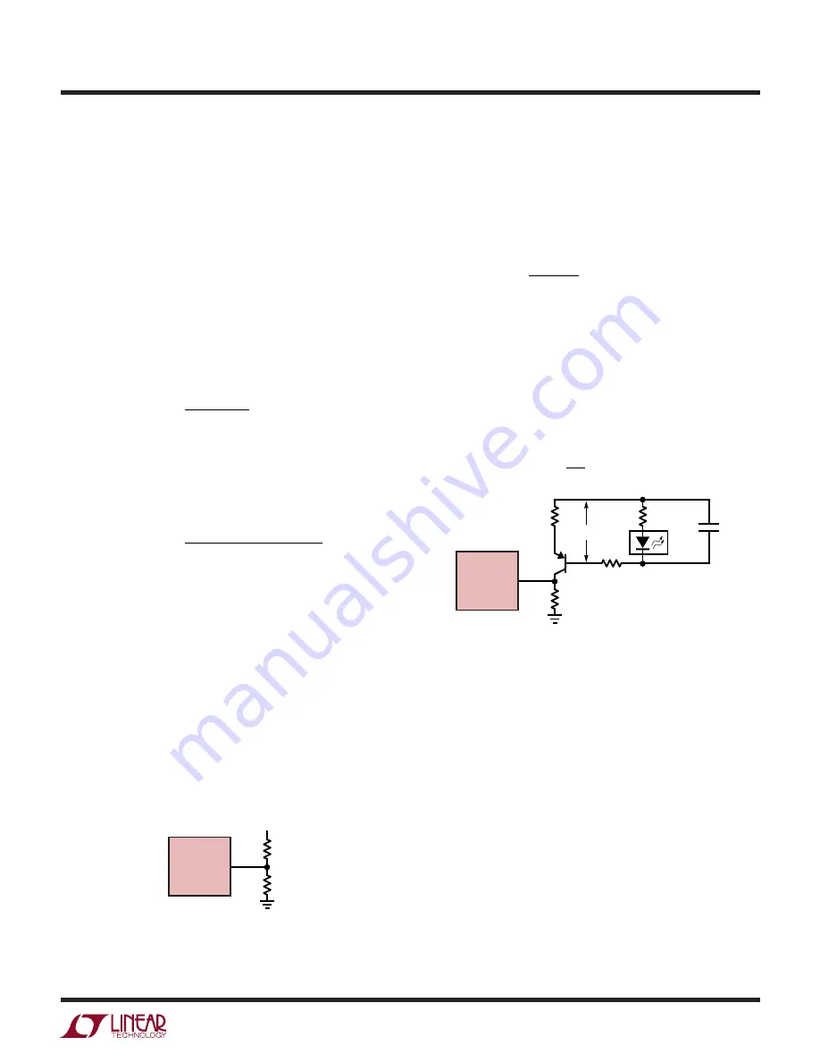
If some level of analog dimming is acceptable at minimum
supply levels, then the CTRL pin can be used with a resistor
divider to V
IN
(as shown on page 1) to provide a higher
output current at nominal V
IN
levels.
FB
LT3956
V
OUT
R4
3956 F02
R3
Figure 2. Feedback Resistor Connection
for Boost or SEPIC LED Drivers
FB
LT3956
100k
V
OUT
C
OUT
R4
3956 F03
R3
LED
ARRAY
R
LED
+
–
Figure 3. Feedback Resistor Connection for
Buck Mode or Buck-Boost Mode LED Driver
Programming Output Voltage (Constant-Voltage
Regulation) or Open LED/Overvoltage Threshold
For a boost or SEPIC application, the output voltage can
be set by selecting the values of R3 and R4 (see Figure 2)
according to the following equation:
V
R
R
R
OUT
=
+
1 25
3
4
4
. •
For a boost type LED driver, set the resistor from the output
to the FB pin such that the expected voltage level during
normal operation will not exceed 1.1V. For an LED driver
of buck mode or a buck-boost mode configuration, the
output voltage is typically level-shifted to a signal with
respect to GND as illustrated in Figure 3. The output can
be expressed as:
V
V
R
R
OUT
BE
=
+
1 25
3
4
. •
ISP/ISN Short-Circuit Protection Feature for SEPIC
The ISP and ISN pins have a protection feature indepen-
dent of the LED current sense feature that operates at
ISN below 3V. The purpose of this feature is to provide
continuous current sensing when ISN is below the LED
current sense common mode range (during start-up or
an output short-circuit fault) to prevent the development
of excessive switching currents that could damage the
power components in a SEPIC converter. The action
threshold (335mV, typ) is above the default LED current
sense threshold, so that no interference will occur over
the ISN voltage range where these two functions overlap.
This feature acts in the same manner as switch-current
limit — it prevents switch turn-on until the ISP/ISN differ-
ence falls below the threshold.