


QUICK START GUIDE FOR DEMONSTRATION CIRCUIT 1317A-F
ACTIVE RESET ISOLATED 9-36V INPUT TO 3.3V @20A DC/DC POWER CONVERTER
3
Figure 2. Scope Probe Placement for Measuring Input or Output Ripple
ACTIVE RESET CIRCUIT
The Active Reset circuit on DC1317A-F demo board
consists of a small P-Channel MOSFET Q13 and
reset capacitor C25. The MOSFET Q13 is used to
connect the reset capacitor across the transformer
T1 primary winding during the reset period when
Q1 MOSFET is off. The voltage across capacitor
C25 automatically adjusts with the duty cycle to
provide complete transformer reset under all oper-
ating conditions.
Also the active reset circuit shapes the reset voltage
into a square waveform that results in lower drain
voltages for Q1 and Q2 MOSFETs. The lower
MOSFET drain voltages allow lower voltage and
lower Rdson MOSFETs to be used. The MOSFETs
must be avalanche rated for the peak reset voltage.
If non-avalanche rated MOSFETs are used a proper
drain voltage derating should be used.
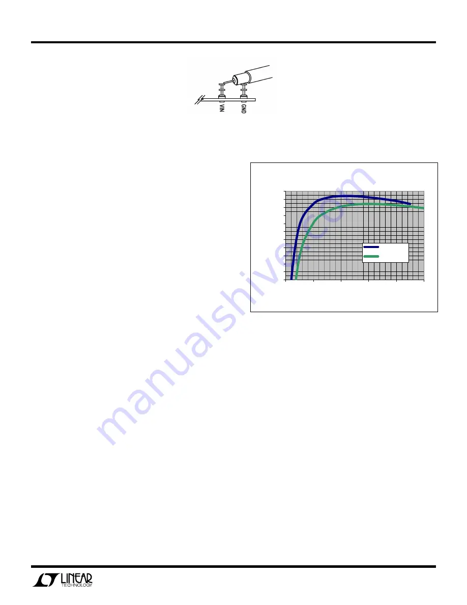
The main benefit of active reset circuit in the case of
DC1317A-F demo board is high efficiency (shown
in Figure 3), wide input range, high power density
and small size. To achieve such high efficiency all of
the power components were carefully selected.
Please consult LT factory for assistance if any
changes to the circuit are required.
DC1317A-F (LT1952) 3.3V Output Efficiency
72%
74%
76%
78%
80%
82%
84%
86%
88%
90%
92%
94%
0
5
10
15
20
25
Iout [A]
E
ff
ic
ie
nc
y
12V input
24V input
Figure 3. High efficiency of DC1317A-F allows the
board to be used in thermally critical applications
OUTPUT LOAD STEP RESPONSE
The load step response of DC1317A-F is very fast
even though relatively small amount of output ca-
pacitance is present (200uF ceramic and 470uF
electrolytic). This is thanks to fast error amplifier of
LT4430, optimal amount of current slope compen-
sation of LT1952, fast opto coupler and fast error
amplifier of LT1952. If higher load steps need to be
handled more output capacitance can be added in
order to keep the voltage transients at the desired
level. The load step transients are shown in Figure
4.