8
dc2581af
DEMO MANUAL DC2581A
DC2581A SETUP
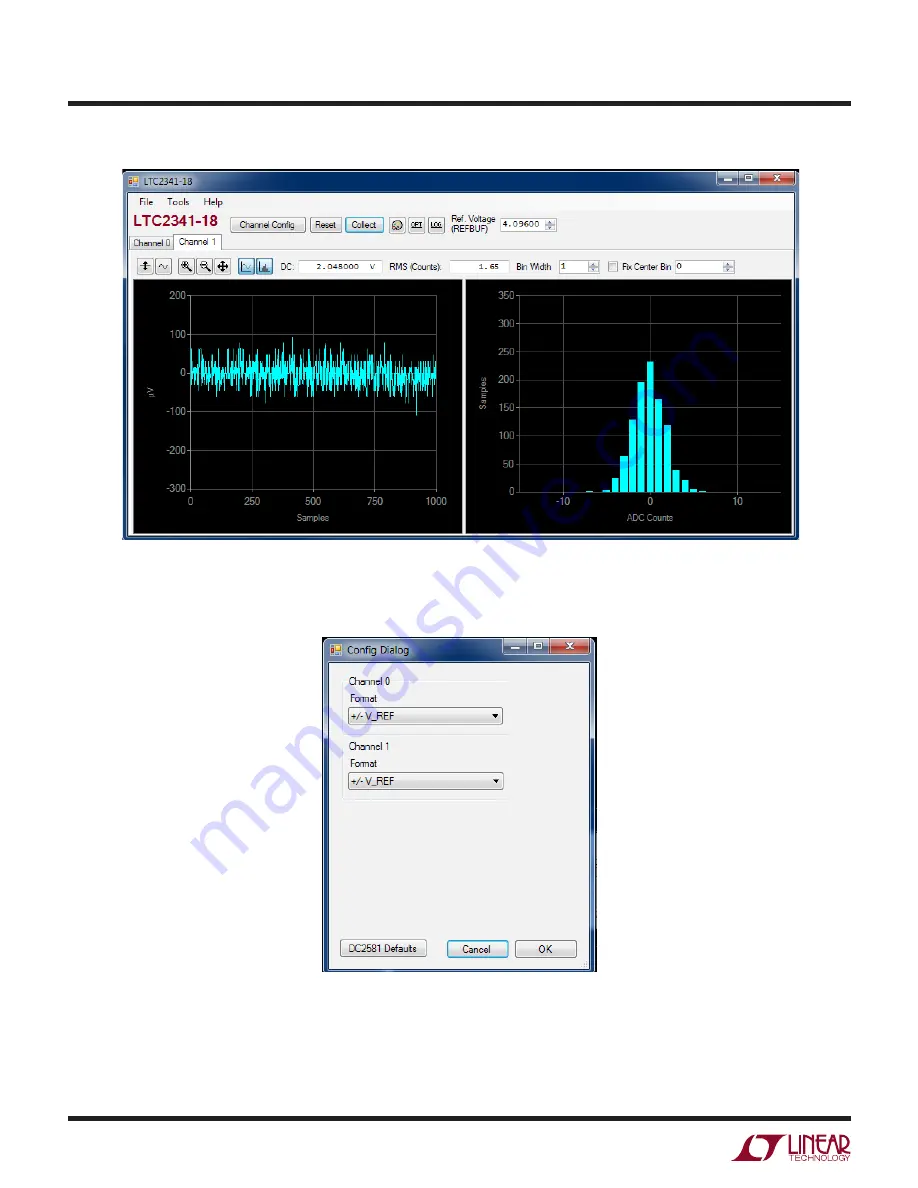
Figure 6. QuikEval Screen Shot
Figure 7. QuikEval Configuration Menu
Page 1: ...he DC590 DC2026 and DC890 data collection boards Use the DC590 DC2026 to L LT LTC LTM Linear Technology and the Linear logo are registered trademarks and PScope QuikEval and SoftSpan are trademarks of Linear Technology Corporation All other trademarks are the property of their respective owners demonstrate DC performance such as peak to peak noise and DC linearity Use the DC890 if precise sampling...
Page 2: ... The PScope software should recognize the DC2581A and configure itself automatically Click the Collect button See Figure 3 to begin acquiring data The Collect button then changes to Pause which can be clicked to stop data acquisition DC590 DC2026 QUICK START PROCEDURE IMPORTANT To avoid damage to the DC2581A make sure that VCCIO JP6 of the DC590 JP3 of the DC2026 of the DC590 DC2026 is set to 3 3V...
Page 3: ...refore it is recommended for lower sample rates to divide down a higher frequency clock to the desired sample rate The ratio of clock frequency to conversion rate is shown in the Assembly Options table If theclockinputistobedrivenwithlogic itisrecommended that the 49 9Ω termination resistor R4 be removed Driving R4 with discrete logic may result in slow rising edges Theseslowrisingedgesmaycompromi...
Page 4: ...n the Set Demo Bd Options button in the PScope tool bar shown in Figure 4 This will open the Configure Channels menu of Figure 5 In this menu it is possible to set the input signal range setting for each channel There is also a button to return PScope to the default DC2581A settings which are optimized for the default hardware settings of the DC2581A Thereareanumberofscenariosthatcanproducemislead...
Page 5: ...of a symmetricallayoutaroundtheanaloginputswillminimize theeffectsofparasiticelements Shieldanaloginputtraces with ground to minimize coupling from other traces Keep traces as short as possible Component Selection When driving a low noise low distortion ADC such as the LTC2341 component selection is important so as to not degrade performance Resistors should have low values to minimize noise and d...
Page 6: ...6 dc2581af DEMO MANUAL DC2581A DC2581A SETUP Figure 3 PScope Screen Shot Figure 4 PScope Tool Bar ...
Page 7: ...7 dc2581af DEMO MANUAL DC2581A DC2581A SETUP Figure 5 PScope Configuration Menu ...
Page 8: ...8 dc2581af DEMO MANUAL DC2581A DC2581A SETUP Figure 6 QuikEval Screen Shot Figure 7 QuikEval Configuration Menu ...
Page 9: ...s CMOS Only CMOS is currently supported Definitions P1 DC890 interface is used to communicate with the DC890 controller J1 CLK provides the master clock for the DC2581A when interfaced to the DC890 J2 FPGA PROGRAM is used to program the FPGA This is for factory use only JP4 EEPROM is for factory use only The default posi tion is WP JP5 JP8 AIN0 AIN1 can be used to short individual AIN inputs to gr...
Page 10: ...UDING ANY WARRANTY OF MERCHANTABILITY OR FITNESS FOR ANY PARTICULAR PURPOSE EXCEPT TO THE EXTENT OF THIS INDEMNITY NEITHER PARTY SHALL BE LIABLE TO THE OTHER FOR ANY INDIRECT SPECIAL INCIDENTAL OR CONSEQUENTIAL DAMAGES The user assumes all responsibility and liability for proper and safe handling of the goods Further the user releases LTC from all claims arising from the handling or use of the goo...