1
dc2530af
DEMO MANUAL DC2530A
DESCRIPTION
LT8640S
42V, 6A Micropower Synchronous
Step-Down Silent Switcher 2
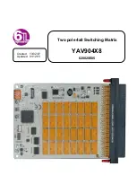
Demonstration circuit 2530A is a 42V, 6A micropower syn-
chronous step-down second generation Silent Switcher
®
with spread spectrum frequency modulation featuring
the
LT8640S
. The demo board is designed for 5V output
from a 5.8V to 42V input. The wide input range allows a
variety of input sources, such as automotive batteries and
industrial supplies. The LT8640S is a compact, ultralow
emission, high efficiency, and high speed synchronous
monolithic step-down switching regulator. The integrated
bypass capacitors optimize all the fast current loops and
make it easier to minimize EMI/EMC emissions by reduc-
ing layout sensitivity. Selectable spread spectrum mode
can further improve EMI/EMC performance. Ultralow qui-
escent current in Burst Mode
®
operation achieves high
efficiency at very light loads. Fast minimum on-time of
30ns enables high V
IN
to low V
OUT
conversion at high
frequency.
The LT8640S switching frequency can be programmed
either via oscillator resistor or external clock over a
200kHz to 3MHz range. The default frequency of demo
circuit 2530A is 2MHz. The SYNC pin on the demo board
is grounded (JP1 at BURST position) by default for low
ripple Burst Mode operation. To synchronize to an external
clock, move JP1 to SYNC and apply the external clock to
the SYNC terminal. Spread spectrum mode and forced
continuous mode can be selected respectively by moving
JP1 shunt. Figure 1 shows the efficiency of the circuit at
12V input and 24V input in Burst Mode Operation (input
from VIN terminal to bypass the EMI filter). Figure 2 shows
L
, LT, LTC, LTM, Linear Technology, the Linear logo, Burst Mode and Silent Switcher are
registered trademarks of Analog Devices, Inc. All other trademarks are the property of their
respective owners.
PERFORMANCE SUMMARY
the LT8640S temperature rising on DC2530A demo board
under different load conditions. The rated maximum load
current is 6A, while derating is necessary for certain input
voltage and thermal conditions.
The demo board has an EMI filter installed. The EMI
performance of the board (with EMI filter) is shown on
Figure 3. The red line in Radiated EMI Performance is
CISPR25 Class 5 peak limit. The figure shows that the
circuit passes the test with a wide margin. To achieve EMI/
EMC performance as shown in Figure 3, the input EMI
filter is required and the input voltage should be applied
at VEMI terminal. An inductor can be added in the EMI
filter to further reduce the conducted emission. The EMI
filter can be bypassed by applying the input voltage at
VIN terminal.
The LT8640S data sheet gives a complete description of
the part, operation and application information. The data
sheet must be read in conjunction with this demo manual
for demo circuit 2530A. The LT8640S is assembled in a
4mm × 4mm LQFN package with exposed pads for low
thermal resistance. The layout recommendations for low
EMI operation and maximum thermal performance are
available in the data sheet section Low EMI PCB Layout
and Thermal Considerations and Peak Output Current.
Design files for this circuit board are available at
http://www.linear.com/demo/DC2530A
Specifications are at T
A
= 25°C
SYMBOL PARAMETER
CONDITIONS
MIN
TYP
MAX
UNITS
V
IN_EMI
Input Supply Range with EMI Filter
5.8
42
V
V
OUT
Output Voltage
4.85
5
5.15
V
I
OUT
Maximum Output Current
Derating is Necessary for Certain V
IN
and Thermal Conditions
6
A
f
SW
Switching Frequency
1.85
2
2.15
MHz
EFF
Efficiency
V
IN
= 12V, I
OUT
= 3A
94.3
%


