


2
dc1861af
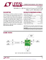
DEMO MANUAL DC1861A
QUICK START PROCEDURE
1. Connect all test equipment as shown in Figure 1.
2. Set the power supply output voltage to 3.3V, and set
the current limit to 150mA.
3. Connect the V
CC
pin to the 3.3V supply. Connect EN
to the 3.3V supply.
BE SURE TO CONNECT THE V
CC
PIN
BEFORE
THE EN PIN TO ENSURE THAT THE PART
DOES NOT GET DAMAGED. ALSO, REMOVE POWER
FROM EN PIN
BEFORE
REMOVING POWER FROM
THE V
CC
PIN.
4. Set the LO signal generator to provide a 1800MHz CW
signal at about 0dBm to the demo board’s LO port.
5. Set the RF signal generators to provide one 1950MHz
CW signal and one 1951MHz CW signal. The signals
should be applied to the 2-way combiner. The output
of the combiner should be applied to the demo board’s
RF input port. The two tones should be set to about
–6dBm each at the mixer’s RF input port.
6. Set the spectrum analyzer’s center frequency to 150MHz.
7. Perform various measurements (Conversion Gain, OIP3,
LO leakage, etc.)
PARTS LIST
NOTES ON TEST EQUIPMENT AND SETUP
• High performance signal generators with low harmonic
outputs should be used for 2-tone measurements. Oth-
erwise, lowpass filters at the signal generator outputs
should be used to suppress harmonics.
• High quality combiners should be used to present a
broadband 50Ω termination on all ports as well as pro-
vide good port-to-port isolation. Attenuator pads may
be used on the inputs to the combiner and the RF input
port of the LTC5567 mixer shown in Figure 1. Adding
attenuator pads further improves source isolation and
helps prevent the signal generators from producing
intermodulation products.
• Spectrum analyzers can produce significant internal
distortion products if they are overdriven. Generally,
spectrum analyzers are designed to operate at their
best with about –30dBm to –40dBm at their input. The
spectrum analyzer’s input attenuation setting should
be used to avoid saturating the instrument. Set the
spectrum analyzer’s input attenuation depending on
the spectrum analyzer used.
• Before performing measurements on the DUT, the sys-
tem performance should be evaluated to ensure that
a clean input signal is obtained and that the spectrum
analyzer’s internal distortion is minimized.
ITEM
QTY
REFERENCE
PART DESCRIPTION
MANUFACTURER/PART NUMBER
1
2
C1, C2
CAP, X7R, 0.01μF, 25V, 10%, 0402
AVX, 04023C103KAT
2
1
C3
CAP, NPO, 2.7pF, 50V, 5%, 0402
AVX, 04025A2R7JAT
3
0
C4, C6
TBD, 0402
4
1
C5
CAP, NPO, 3.9pF, 50V, 5%, 0402
AVX, 04025A3R9JAT
5
2
C7, C8
CAP, NPO, 330pF, 16V, 5%, 0402
AVX, 0402YA331JAT
6
1
C9
CAP, X7R, 1μF, 10V, 10%, 0603
AVX, 0603ZC105KAT
7
4
E1-E4
TESTPOINT, TURRET, 0.063" PBF
MILL-MAX, 2308-2-00-80-00-00-07-0
8
4
J1-J4
CONN, SMA, 50Ω EDGE-LANCH
E. F. JOHNSON, 142-0701-851(PBF)
9
2
L1, L2
INDUCTOR, WIREWOUND, 300nH, ±5%, 0603
COILCRAFT, 0603HP-R30XJLW
10
2
R1, R2
RES, CHIP, 3.01k, 1/16W, 1% 0402
VISHAY, CRCW04023K01FKED
11
0
R3
TBD, 0402
12
1
R4
RES, CHIP, 0Ω, 0603
NIC NRC060000TRF
13
1
T1
RF TRANSFORMER, TC8-1-10LN+
MINI-CIRCUITS, TC8-1-10LN+
14
1
U1
I.C. LTC5567IUF, QFN 16 PIN, 4mm
×
4mm
LINEAR TECH. INC., LTC5567IUF