background image

2

dc1759af

DEMO MANUAL DC1759A

 QUICK START PROCEDURE

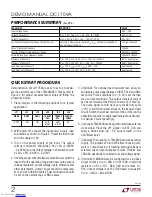
Demonstration circuit 1759A is easy to set up to evalu-
ate the performance of the LTM4620AEV. Please refer to 
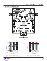
Figure 2 for proper measurement setup and follow the 
procedure below:

1. Place jumpers in the following positions for a typical 

application:

JP1

JP2

JP3

JP4

JP5

JP6

MODE

RUN1

RUN2

TRACK1 

SEL.

TRACK2 

SEL.

CLKOUT 

PHASE

CCM

ON

ON

SOFT-

START

SOFT-

START

90°

2. With power off, connect the input power supply, load 

and meters as shown in Figure 2. Preset the load to 0A 
and V

IN

 supply to 12V.

3. Turn on the power supply at the input. The output 

voltage in channel 1 should be 3.3V ±1.5% (3.2505V 
~ 3.3495V) and the output voltage in channel 2 should 
be 5V ±1.5% (4.925V ~ 5.075V).

4.  Once the proper output voltage is established, adjust the 

load within the operating range and observe the output 
voltage regulation, output voltage ripple, efficiency and 
other parameters. Output ripple should be measured 
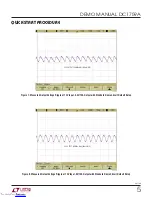
at J1 and J2 with BNC cables. 50Ω termination should 
be set on the oscilloscope or BNC cables.

5. (Optional) For optional load transient test, apply an 

adjustable pulse signal between IOSTEP CLK and GND 
test point. Pulse amplitude (3V ~ 3.5V) sets the load 
step current amplitude. The output transient current 
can be monitored at the BNC connector J3 (15mV/A). 
The pulse signal should have very small duty cycle 
(<1%) to limit the thermal stress on the transient load 
circuit. Switch the jumper resistors R34 or R35 (on the 
backside of boards) to apply load transient on channel 1 
or channel 2 correspondingly.

6.  (Optional) LTM4620A can be synchronized to an external 

clock signal. Place the JP1 jumper on EXT_CLK and 
apply a clock signal (0V ~ 5V, square wave) on the 
CLKIN test point.

7.  (Optional) The outputs of LTM4620A can track another 

supply. The jumpers JP4 and JP5 allow choosing soft-
start or output tracking. If tracking external voltage is 
selected, the corresponding test points, TRACK1 and 
TRACK2, need to be connected to a valid voltage signal.

8. (Optional) LTM4620A can be configured for a 2-phase 

single output at up to 26A on DC1759A. Install 0Ω 
resistors on R14, R17, R28, R39 and remove R7, 
R19. Output voltage is set by R25 based on equation 
V

OUT

 = 0.6V(1 + 60.4k/R25).

 PERFORMANCE SUMMARY

PARAMETER

CONDITION

VALUE

Input Voltage Range

5.5V ~ 16V

Output Voltage V

OUT1

V

IN

 = 5.5V ~ 16V, I

OUT1

 = 0A ~ 13A, JP1: CCM

3.3V ±1.5%

Output Voltage V

OUT2

V

IN

 = 5.5V ~16V, I

OUT2

 = 0A ~ 13A, JP1: CCM

5V ±1.5%

Per-Channel Maximum Continuous Output Current

Derating is Necessary for Certain V

IN

, V

OUT

 and Thermal Conditions, 

See Data Sheet for Detail.

13A (per-Channel)

Default Operating Frequency

750kHz

Resistor Programmable Frequency Range

250kHz to 780kHz

External Clock Sync. Frequency Range

400kHz to 780kHz

Efficiency of Channel 1

V

IN

 = 12V, V

OUT1

 = 3.3V, I

OUT1

 = 13A, f

SW

 = 750kHz

91.7% See Figure 3

Efficiency of Channel 2

V

IN

 = 12V, V

OUT2

 = 5V, I

OUT2

 = 13A, f

SW

 = 750kHz

93.8% See Figure 4

Load Transient of Channel 1

V

IN

 = 12V, V

OUT1

 = 3.3V, I

SETP

 = 6.5A ~ 13A

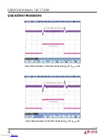
See Figure 5

Load Transient of Channel 2

V

IN

 = 12V, V

OUT2

 = 5V, I

SETP

 = 6.5A ~ 13A

See Figure 6

(T

A

 = 25°C)

Downloaded from

Arrow.com.

Downloaded from

Arrow.com.

Summary of Contents for DC1759A

Page 1: ... 26A output solution with optional jumper resistors The board allows the user to program how its output ramps up and L LT LTC LTM Linear Technology the Linear logo and Burst Mode are registered trademarks of Linear Technology Corporation All other trademarks are the property of their respective owners down through the TRACK SS pin The output can be set up to either coincidentally or ratiometricall...

Page 2: ...istors R34 or R35 on the backsideofboards toapplyloadtransientonchannel1 or channel 2 correspondingly 6 Optional LTM4620Acanbesynchronizedtoanexternal clock signal Place the JP1 jumper on EXT_CLK and apply a clock signal 0V 5V square wave on the CLKIN test point 7 Optional The outputs of LTM4620A can track another supply The jumpers JP4 and JP5 allow choosing soft start or output tracking If track...

Page 3: ... 2 VOUT2 5V fSW 750kHz Channel 1 Disabled LOAD CURRENT A 0 EFFICIENCY 100 90 80 95 85 75 4 8 2 6 10 dc1759a F03 13 12 3 7 1 5 9 11 VIN 5 5V VOUT1 3 3V VIN 12V VOUT1 3 3V VIN 16V VOUT1 3 3V LOAD CURRENT A 0 EFFICIENCY 100 90 80 95 85 75 4 8 2 6 10 dc1759a F04 13 12 3 7 1 5 9 11 VIN 5 5V VOUT2 5V VIN 12V VOUT2 5V VIN 16V VOUT2 5V Downloaded from Arrow com Downloaded from Arrow com Downloaded from Ar...

Page 4: ...E Figure 5 Measured Channel 1 6 5A to 13A Load Transient VIN 12V VOUT1 3 3V Figure 6 Measured Channel 2 6 5A to 13A Load Transient VIN 12V VOUT2 5V dc1759a F05 3 3V OUTPUT 20MHz BW 100mV DIV 6 5A TO 13A LOAD Downloaded from Arrow com Downloaded from Arrow com Downloaded from Arrow com Downloaded from Arrow com ...
Page 5: ...V Input 3 3V 13A Output with Standard Demo Circuit Default Setup Figure 8 Measured Output Voltage Ripple at 12V Input 5V 13A Output with Standard Demo Circuit Default Setup dc1759a F08 5V OUTPUT 20MHz BW 20mV DIV Downloaded from Arrow com Downloaded from Arrow com Downloaded from Arrow com Downloaded from Arrow com Downloaded from Arrow com ...

Page 6: ...rmal Capture at 12VIN 3 3VOUT at 13A and 5VOUT at 13A Ambient Temperature 23 C 200LFM Airflow and No Heat Sink Downloaded from Arrow com Downloaded from Arrow com Downloaded from Arrow com Downloaded from Arrow com Downloaded from Arrow com Downloaded from Arrow com ...

Page 7: ...Res Chip 13 3k 1 0603 VISHAY CRCW060313K3FKED 18 1 R30 Res Chip 191k 1 0603 VISHAY CRCW0603191KFKED 19 1 R34 Res Chip 0Ω 0 5W 2010 TEPRO RN6083 20 1 R37 Res Chip 0 015Ω 2W 2512 VISHAY WSL2512R0150FEA 21 1 U1 LTM4620AEV 15X15X4 41 LGA LINEAR TECH LTM4620AEV Additional Circuits 22 0 COUT2 COUT3 COUT6 COUT8 OPT 1210 OPT 23 0 C1 OPT 0805 OPT 24 0 C3 C4 C8 C10 C11 C12 OPT 0603 OPT 25 0 R2 R4 R6 R8 R11 ...

Page 8: ...T LINEAR TECHNOLOGY APPLICATIONS ENGINEERING FOR ASSISTANCE THIS CIRCUIT IS PROPRIETARY TO LINEAR TECHNOLOGY AND SCHEMATIC SUPPLIED FOR USE WITH LINEAR TECHNOLOGY PARTS SCALE NONE www linear com 2 Thursday November 15 2012 1 2 HIGH EFFICIENCY DUAL 13A STEP DOWN MODULE REGULATOR LT JIAN L N A LTM4620AEV DEMO CIRCUIT 1759A E4 E4 J6 J6 R16 OPT R16 OPT J7 J7 JP3 OFF RUN2 JP3 OFF RUN2 1 3 2 E15 TEMP E1...

Page 9: ...LE OPERATION IN THE ACTUAL APPLICATION COMPONENT SUBSTITUTION AND PRINTED CIRCUIT BOARD LAYOUT MAY SIGNIFICANTLY AFFECT CIRCUIT PERFORMANCE OR RELIABILITY CONTACT LINEAR TECHNOLOGY APPLICATIONS ENGINEERING FOR ASSISTANCE THIS CIRCUIT IS PROPRIETARY TO LINEAR TECHNOLOGY AND SCHEMATIC SUPPLIED FOR USE WITH LINEAR TECHNOLOGY PARTS SCALE NONE www linear com 2 Thursday November 15 2012 2 2 HIGH EFFICIE...

Page 10: ...HALL BE LIABLE TO THE OTHER FOR ANY INDIRECT SPECIAL INCIDENTAL OR CONSEQUENTIAL DAMAGES The user assumes all responsibility and liability for proper and safe handling of the goods Further the user releases LTC from all claims arising from the handling or use of the goods Due to the open construction of the product it is the user s responsibility to take any and all appropriate precautions with re...

Reviews: