- 22 -
BLOCK DIAGRAM DESCRIPTION
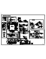
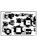
1. Video controller unit and display data conversion unit
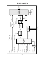
The video controller unit receives the video signal inputted to the tuner, AV port (AV1, AV2, S-Video and
component) and converts it to the analog RGB signal through the microcomputer (VCTI) combined with the
video decoder that integrates various functions in one chip.
Then, it is inputted to the AD converter (AD9883) and generates the 4:4:4 format digital signal. This digital signal
is inputted to the picture enhancer (FLI2300), which processes the video signal and converts the image quality
enhanced data to an analog RGB signal again before displaying it.
The image quality enhanced de-interlace signal is inputted to the scaler (GM5221) and converted to the LVDS
signal by the integrated LVDS IC before being sent to the LCD module.
VCTI is the main microcomputer that processes both video signals and sound signals. It also processes the RF
signal received from the tuner.
The scaler enables to adjust timing on the LCD panel, as well as an adjustment of the size and position of the
input signal.
The graphic controller unit receives the PC (analog RGB) input and the DVI-D (digital signal), and sends the PC
input to the scaler analog port and DVI-D input to the digital port.
The scaler receives two inputs and converts them to the LVDS signal before sending to the module.
2. Power unit
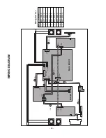
The power unit supplies 33V, 24V and 12V DC power to the main board. 33V DC power is used for the tuner,
whereas 24V DC power is directly used by the inverter and the sound amplifier IC. 24V DC power is also used
to generate 5V through the regulator. 12V DC power is used for the LCD panel.
5V DC is converted to 3.3V and 1.8V through the regulator, which supplies the necessary power to various ICs,
such as VCTI, scaler, FLI2300 and AD9883.

