5-27
4. OPTICAL POWER SETTING
<Test for checking DVD LD and CD LD>
When you change the Travers ass°Øy(including pick-up) or loader PCB, you must do the laser power setting to match
pick-up and loader PCB.
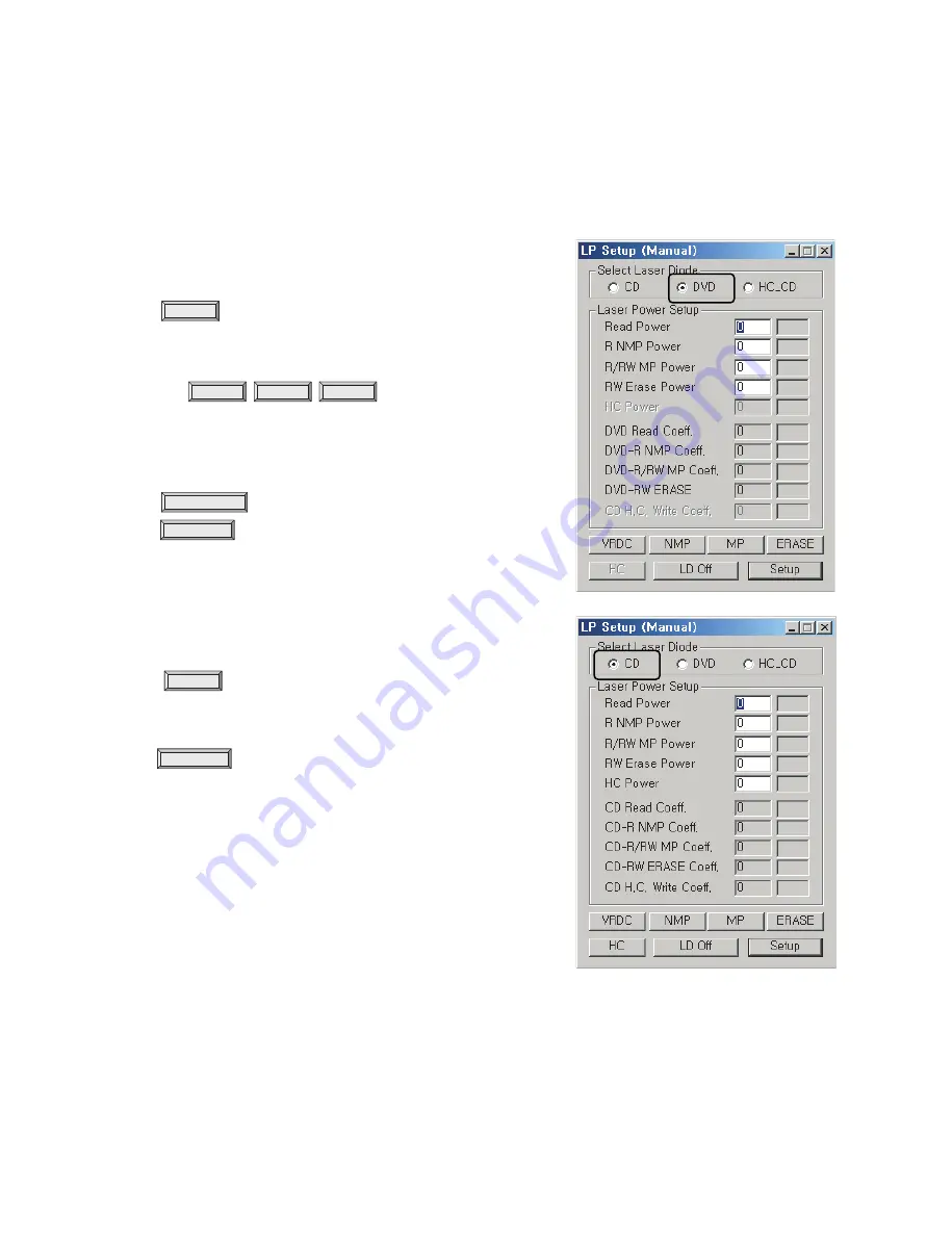
1) DVD LD power setting
• Select the DVD in the ‘Select Laser Diode’
• Press (Read Power On, Strong Read light)
• Measure optical read Power.
• Write read power value.
• In case of ,
you are able to measure the power through same procedure.
(caution) Don’t watch light directly.
• When you finish optical power measurement,
press button(LD Off).
• Press button.(save to ERPROM)
2) CD LD Power Setting
• Select the CD in the ‘Select Laser Diode’
• Press .
•Measure optical read Power.
•Write Read Power value.
•Press button(save to ERPROM)
*** In case of CD power setting of RS-01A, loader don’t need to set up
write power.
Although NMP, MP,Erase and HC power is N.G when you press setup,
please ignore the N.G message.
Because of RS-01A only support reading function about CD-R/RW.
* Look at reference sheet to test Optical Power.
**Power value is ß— unit. Value is read power X 100.
VRDC
VRDC
NMP
MP
ERASE
LD Off
Setup
Setup
Summary of Contents for RC-185
Page 1: ...SERVICE MANUAL LG RC 185 MODEL ...
Page 52: ...3 56 3 57 PRINTED CIRCUIT DIAGRAMS 1 VCR P C BOARD TOP VIEW ...
Page 53: ...3 58 3 59 2 VCR P C BOARD BOTTOM VIEW ...
Page 54: ...3 60 3 61 3 SMPS P C BOARD 4 HDMI P C BOARD HDMI MODEL ONLY TOP VIEW BOTTOM VIEW ...
Page 55: ...3 62 3 63 5 KARAOKE P C BOARD KARAOKE MODEL ONLY ...
Page 56: ...3 64 3 65 6 KEY P C BOARD 8 TOOL 9 TOOL 7 TOOL ...
Page 57: ......
Page 84: ...3 100 3 101 PRINTED CIRCUIT DIAGRAMS 1 VDR P C BOARD TOP VIEW ...
Page 85: ...3 102 3 103 2 VDR P C BOARD BOTTOM VIEW ...
Page 117: ......
Page 134: ...5 17 2 DISC SPECIFICATION 3 DISC MATERIALS 1 DVD ROM Single Layer Dual Layer ...
Page 159: ......
Page 160: ...5 42 5 43 CIRCUIT DIAGRAMS 1 DSP CIRCUIT DIAGRAM A B C D E F G H I J K L M N O P Q R S T ...
Page 161: ...5 44 5 45 2 RF CIRCUIT DIAGRAM A B C D E F G H I J K L M N O P Q R S T ...
Page 162: ...5 46 5 47 3 DRIVE CIRCUIT DIAGRAM A B C D E F G H I J K L M N O P Q R S T ...
Page 164: ...5 50 5 51 PRINTED CIRCUIT DIAGRAMS 1 MAIN P C BOARD TOP VIEW ...


