background image

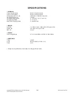
SPECIFICATIONS

 1-9

• GENERAL

Power requirements  

Refer to the main label.

Power consumption  

Refer to the main label.

Dimensions (W x H x D)  

395.5 mm x 548 mm x 446 mm

Net Weight (Approx.)  

16.5 kg

Operating temperature  

5 °C to 35 °C (41 °F to 95 °F)

Operating humidity  

5 % to 90 %

Bus Power Supply (USB)  

5 V     500 mA

• INPUTS

AUX IN  

1.2 Vrms (1 kHz, 0 dB, 600 

Ω

, RCA jack, L/R)

PORT. IN  

0.8 Vrms (3.5 ø jack, L/R)

MIC. IN 

25 mV

• TUNER

FM Tuning Range  

87.5 to 108.0 MHz or 87.50 to 108.00 MHz

• AMPLIFIER

Total  

400 W

Front  

Mono 400 W (at 1 kHz, 4 

Ω

)

THD  

20 %

Š

 Design and specifications are subject to change without notice.

Summary of Contents for OM5541

Page 1: ...em SERVICE MANUAL MODEL OM5541 CAUTION BEFORE SERVICING THE UNIT READ THE SAFETY PRECAUTIONS IN THIS MANUAL MODEL OM5541 SERVICE MANUAL P NO AFN76793367 SEPTEMBER 2014 Website http biz lgservice com Internal Use Only ...

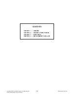
Page 2: ...CONTENTS SECTION 1 GENERAL SECTION 2 CABINET MAIN CHASSIS SECTION 3 ELECTRICAL SECTION 4 REPLACEMENT PARTS LIST 1 1 ...

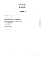
Page 3: ...N 1 SUMMARY CONTENTS ESD PRECAUTIONS 1 3 HIDDEN KEY MODE 1 4 SERVICE INFORMATION FOR EEPROM 1 5 PROGRAM DOWNLOAD UPDATE GUIDE 1 6 1 MICOM PROGRAM 1 6 2 MCS PROGRAM 1 7 3 EQ PROGRAM 1 8 SPECIFICATIONS 1 9 1 2 ...

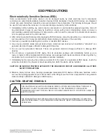
Page 4: ... damage ESD devices 5 Do not use freon propelled chemicals These can generate electrical charges sufficient to damage ESD devices 6 Do not remove a replacement ESD device from its protective package until immediately before you are ready to install it Most replacement ESD devices are packaged with leads electrically shorted together by conductive foam aluminum foil or comparable conductive materia...

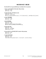
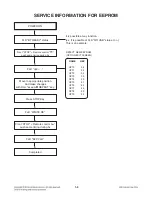
Page 5: ...ROM Option by SKIP 3 Clear EEPROM Front Key STOP RCU Key SKIP 4 Edit EEPROM Front Key STOP RCU Key SKIP You can change the digit of option by SKIP You can edit 0 f by REPEAT or PLAY PAUSE key 5 Bluetooth DUT Front Key STOP RCU Key PROGRAM Bluetooth model only 6 Power Disc Lock On Off CD Function Only Active Front Key STOP RCU Key EQ 7 Amp Clip On Off Front Key STOP RCU Key Mute Amp Clip Mode Chang...

Page 6: ...me timing during 5s FLD op0 Move to appropriate position And make changes with Rmc REPEAT key Press STOP Key FLD WRITE OK Front STOP Remote control push same timing during 5s FLD E2P CLR Completed NAME OPT0 OPT1 OPT2 OPT3 OPT4 OPT5 OPT6 OPT7 OPT8 OPT9 DETECT NEW EEPROM OPTION EDIT SCREEN HEX 09 00 00 00 00 21 83 45 00 00 1 5 SERVICE INFORMATION FOR EEPROM ...

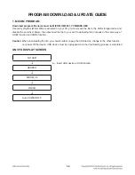
Page 7: ...he file to your set Downloading file proceeds in the same way at USB1 function and USB2 function Caution When downloading the file you should neither unplug the USB device change to the other function nor power off the device USB device must be unplugged when the downloading process is completed ON VFD DISPLAY SCREEN NO USB Insert USB device at USB function SEARCH MICOM UP FINISH Auto POWER OFF 1 ...

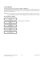
Page 8: ...hen download the file to your set Downloading file proceeds in the same way at USB1 function and USB2 function Caution When downloading the file you should neither unplug the USB device change to the other function nor power off the device USB device must be unplugged when the downloading process is completed ON VFD DISPLAY SCREEN NO USB Insert USB device at USB function SEARCH FIRMWARE FINISH Aut...

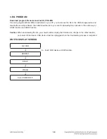
Page 9: ...wnload the file to your set Downloading file proceeds in the same way at USB1 function and USB2 function Caution When downloading the file you should neither unplug the USB device change to the other function nor power off the device USB device must be unplugged when the downloading process is completed ON VFD DISPLAY SCREEN NO USB Insert USB device at USB function SEARCH EQ UP FINISH Auto POWER O...

Page 10: ...Operating temperature 5 C to 35 C 41 F to 95 F Operating humidity 5 to 90 Bus Power Supply USB 5 V 500 mA INPUTS AUX IN 1 2 Vrms 1 kHz 0 dB 600 Ω RCA jack L R PORT IN 0 8 Vrms 3 5 ø jack L R MIC IN 25 mV TUNER FM Tuning Range 87 5 to 108 0 MHz or 87 50 to 108 00 MHz AMPLIFIER Total 400 W Front Mono 400 W at 1 kHz 4 Ω THD 20 Design and specifications are subject to change without notice ...

Page 11: ...1 10 ...

Page 12: ...SECTION 2 CABINET MAIN CHASSIS CONTENTS EXPLODED VIEWS 2 3 1 CABINET AND MAIN FRAME SECTION OM5541 2 3 2 PACKING ACCESSORY SECTION 2 5 2 1 ...

Page 13: ...2 2 ...

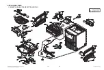
Page 14: ... 261 264 255 270 262 263 265 A47 A46 251 253 291 513 513 A51 A51 464 464 464 464 464 512 514 512 512 512 512 514 512 464 512 512 A43 A48 A49 A44 A42 254 A53 252 CABLE3 CABLE1 CABLE2 464 464 464 464 464 464 464 464 464 464 NOTES THE EXCLAMATION POINT WITHIN AN EQUILATERAL TRIANGLE IS INTENDED TO ALERT THE SERVICE PERSONNEL TO THE PRESENCE OF IMPORTANT SAFETY INFORMATION IN SERVICE LITERATURE ...

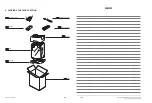
Page 15: ...825 FM Wire Antenna 900 Remote Control 808 Battery 802 Box 801 Instruction Ass y 804 Bag 803 Packing 803 Packing 2 PACKING ACCESSORY SECTION ...

Page 16: ...AGRAM_1 3 27 2 SYSTEM BLOCK DIAGRAM_2 3 29 3 SMPS BLOCK DIAGRAM_1 3 31 4 SMPS BLOCK DIAGRAM_2 3 33 CIRCUIT DIAGRAMS 3 35 1 SMPS CIRCUIT DIAGRAM 3 35 2 MAIN_DSP CIRCUIT DIAGRAM 3 37 3 MAIN_ADC PWM CIRCUIT DIAGRAM 3 39 4 MAIN_AMP CIRCUIT DIAGRAM 3 41 5 FRONT_KEY USB CIRCUIT DIAGRAM 3 43 6 FRONT_VFD CIRCUIT DIAGRAM 3 45 7 FRONT_KEY PTB CIRCUIT DIAGRAM 3 47 8 FRONT_MIC CIRCUIT DIAGRAM 3 49 9 SPK_LED C...

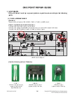
Page 17: ...ermeasure 1 Check if the fuse F901 is open or short circuit 2 Check if the bridge diode BD901 is short circuit by over current with a digital multi meter 3 Check if the NTC thermistor TH901 or TH903 is normal or open Service hint Any picture Remark F901 If F901 is not short circuit replace it with a same specifications one TH901 If TH901 is open replace it with a new one BD901 If BD901 is short ci...

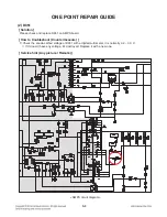
Page 18: ...951 on SMPS board How to troubleshoot Countermeasure 1 Check the anode cathod voltage of D951 with a digital multi meter it is normally 0 2 0 3 V If it doesn t have any voltage it s destroyed Replace it with a new one Service hint Any picture Remark SMPS circuit diagram ...

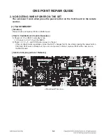
Page 19: ...eshoot Countermeasure 1 Check 5 6 V to CN501 in standby mode If there is no 5 6 V check the SMPS 2 Check 12 V F F and PVDD when power on the set If the set doesn t work regardless of what the KEY1 changes high to low while pressing the power button X500 and X501 work normally but if you can not power on the set replace IC501 with a new one on the MAIN board Service hint Any picture Remark PWR_CTRL...

Page 20: ...eck if IC501 outputs VFD_D0 VFD_CLK and VFD_STB to the FRONT board 3 Check the GR signal pulse signal of IC301 on the FRONT board Check the SG signal pulse signal of IC301 on the FRONT board If the GR and SG signal isn t output replace IC301 with a new one If the GR and SG signal is output replace DIG302 with a new one Service hint Any picture Remark GR signal SG signal Waveform of GR and SG signa...

Page 21: ... for each IC The power is normal but if the signal waveform to the IC is distorted or no signal replace it with a new one 3 Check PVDD If PVDD is abnormal check the SMPS 4 Check 12 V for driving the gate of AMP IC a All the powers are normal but if 12 V is low there is possible for AMP IC to be damaged b Remove L702 L706 one by one When removed a inductance if 12 V is recovered the IC connected to...

Page 22: ... USB D2 from MAIN board to USB board a Check 2 0_D1 signals pin U7 U8 or 1 1_D1 signals pin A7 A8 to IC501on MAIN board b Check USB signals to CN421 pin 2 3 5 6 If there is any trouble check the power for each IC The power is normal but if the signal waveform to the IC is distorted or no signal replace it with a new one 3 Check if Digital audio AMP block on item 4 1 is normal Service hint Any pict...

Page 23: ...e it a new one 4 Check the following I2S signal flow from IC501 to IC601 Refer to item 4 1 If there is any trouble check the power for each IC The power is normal but if the signal waveform to the IC is distorted or no signal replace it with a new one 5 Check if the digital audio AMP block is okay Refer to Digital Audio AMP guide on Item 4 1 If AMP is damaged replace it with a new one Service hint...

Page 24: ...f the tuner control signals CLK DAT CE RST SLT are entered from IC501 to TU500 If it doesn t work replace TUNER with a new one 2 Check if MCS_BCK MCS_LRCK MCS_MCLK are entered from IC501 to IC201 3 Check if ADC_DATA is entered from IC201 to IC501 If no signal check 5 V 3 3 V ADC for IC201 If is NG replace it with a new one 4 Check the following I2S audio signal flow from IC501 to IC601 Refer to it...

Page 25: ... 3 3 V ADC for IC201 If NG replace it a new one 4 Check the following I2S signal flow from IC501 to IC601 Refer to item 4 1 If there is any trouble check the power for each IC The power is normal but if the signal waveform to the IC is distorted or no signal replace it with a new one 5 Check if the digital audio AMP block is okay Refer to Digital Audio AMP guide on Item 4 1 If AMP is damaged repla...

Page 26: ...ntered from IC203 to IC501 If no signal check 5 V 3 3 V ADC for IC203 If NG replace it a new one 6 Check the following I2S signal flow from IC501 to IC601 Refer to item 4 1 If there is any trouble check the power for each IC The power is normal but if the signal waveform to the IC is distorted or no signal replace it with a new one 7 Check if the digital audio AMP block is okay Refer to Digital Au...

Page 27: ...NO Is Vcc 10 V 18 V supplied to IC901 Pin7 D902 normal YES NO Check or replace D902 Is there about 2 5 V at IC941 Pin1 Replace IC941 YES NO D935 normal Replace D935 YES NO D932 normal Replace D932 YES NO D931 normal Replace D931 YES NO D933 D934 normal Replace D933 D934 YES NO Power line of main PCB is short NO 3 12 ELECTRICAL TROUBLESHOOTIHG GUIDE ...

Page 28: ...cc 10 V 18 V supplied to IC911 Pin4 D903 normal YES NO Check or replace D903 Check P CTRL H signal from MCS Check PC902 Q901 normal Replace Q901 Check or replace Q911 YES NO D951 normal Replace D951 YES NO Is there about 2 5 V at IC951 Pin1 Replace IC951 YES NO Q911 base H Power line of main PCB is short NO NO 3 13 ELECTRICAL TROUBLESHOOTIHG GUIDE ...

Page 29: ... Pin4 H Check the P CTL H signal from μ com YES NO Check or replace IC931 No VFD D931 normal Check or replace D931 YES YES NO ZD931 normal Q501 Q502 normal Check or replace ZD931 Check or replace Q501 Q502 YES YES NO NO Check or replace VFD 3 14 ELECTRICAL TROUBLESHOOTIHG GUIDE ...

Page 30: ...8 NO NO Check if IC510 have 3 3 V output Check if IC508 have 1 2 V output X500 32 768 kHz X501 24 MHz Check the operation OK YES YES YES YES YES YES YES 3 IC504 M24C16 CHECK CHECK IC501 PIN Refer to MCS troubleshooting NO Check pinC2 pinB1 DATA CLK Replace MCS NO Check MCS voltage 3 3 VA Check MCS YES OK OK YES NO 3 15 ELECTRICAL TROUBLESHOOTIHG GUIDE ...

Page 31: ...g in usb device Check CN421 NO NO YES Display READ YES Display NO FILE YES Check USB jack CN461 CN462 NO Replace IC501 NO Check IC501 Pin U7 U8 A7 A8 Check usb audio file in usb device MP3 WMA file is playable YES 4 DOUBLE USB FUNCTION 3 16 ELECTRICAL TROUBLESHOOTIHG GUIDE ...

Page 32: ... FL VKK Pin9 3 3 V YES OK NO Check CN400 connection YES Check each Pin voltage YES Check IC400 MC3401 voltage Pin30 VKK 25 8 V Pin13 43 3 3 V YES Check IC501 IC400 data communication STB DATA CLK FLD light on OK NO If voltage is not 3 3 V YES Check IC400 YES NO Replace IC400 NO Check input data IC501 Pin F1 F2 G1 YES OK Check IC501 YES NO Replace IC501 Check output data IC501 Pin D2 YES YES YES 3 ...

Page 33: ...MPS troubleshooting Check X601 12 288 MHz operation NO Replace X601 12 288 MHz Check X601 12 288 MHz OK YES NO Check IC601 Pin21 CLK input Check IC501 MLC3730 Pin B3 RESET Pin A1 SDA Pin A2 SCL output NO Replace R53E R53C R53B Check line resistor output RST R53E SCL R53C SDA R53B NO YES YES YES YES YES YES OK YES A 3 18 ELECTRICAL TROUBLESHOOTIHG GUIDE ...

Page 34: ...4 PWM wave NO Check each line resistor output Check IC601 DATA input NO Check PWM modulator output FL Pin48 49 FR Pin46 47 Other output check NO Replace IC601 Check IC601 NO OK OK YES YES YES YES YES A 3 19 ELECTRICAL TROUBLESHOOTIHG GUIDE ...

Page 35: ... 2 3 48 V YES YES Check IC701 Pin25 26 55 56 input voltage YES Check each line resistor output voltage NO Check IC700 Pin2 6 55 12 V Check IC700 Pin28 29 52 53 input voltage Replace the coil NO Check output line coil Check IC700 Pin4 5 input voltage YES YES YES YES OK 3 20 ELECTRICAL TROUBLESHOOTIHG GUIDE ...

Page 36: ...01 CS5346 Pin41 output data YES YES Check IC201 Pin5 3 3 V Pin14 5 V Check CN501 Pin7 8 5 6 V NO NO Check IC501 MLC3700 input data YES Check IC201 Pin5 3 3 V Pin6 High Pin14 5 V Check IC201 Pin41 SDOUT Pin42 SLCK Pin43 LRCK Pin44 MCLK NO NO IC501 MLC3730 output data Replace IC201 OK YES 3 21 ELECTRICAL TROUBLESHOOTIHG GUIDE ...

Page 37: ...tput Check CN501 pin7 8 5 6 V Replace IC201 NO NO OK YES Check IC420 S4308 pin3 input Check IC420 S4308 pin4 data output Check IC203 AK5358 pin1 2 data input Check IC420 pin6 5 V Check IC203 pin5 5 V pin5 3 3 V Check IC423 pin1 5 V Check IC203 PIN9 SCLK PIN10 MLCK PIN11 LRCK PIN12 ADC_DATA 3 22 ELECTRICAL TROUBLESHOOTIHG GUIDE ...

Page 38: ... SDRAM CLK DATA ADDRESS CS IC502 Pin38 IC502 Pin53 IC502 Pin35 IC203 Pin19 2 AUDIO PATH DAC_MCLK DAC_BCK DAC_LRCK DAC_DATA IC501 Pin D2 IC501 Pin E1 IC501 Pin D1 IC501 Pin E2 3 USB USB_5V D D IC501 Pin A8 IC501 Pin A7 1 2 3 4 5 6 7 8 9 10 ...

Page 39: ...3 24 ...

Page 40: ...P Wire Harness 15P Front KEY 1 FR 1 FFC 29P FFC 10P Wire Harness 12P Wire Harness 7P Front KEY 2 FR 1 FFC 29P FCC 10P FCC 10P USB Wire Harness 12P VFD IR MIC PTB LED AMP 2P MIC IR X_LED Wire Harness 7P Wire Harness 4P Wire Harness 4P Wire Harness 5P Wire Harness 5P WIRING DIAGRAM ...

Page 41: ... SPK LED FRONT2 KST MWOO4MV0 S71W EBL60720702 KEY3 DRV_VBUS2 0 LM37102D USB1 1 USB2 0 OTG 2 0_D D 1 1_D D IR VFD REMOCON Debug_Console_IN OUT JTAG NTRST TDI TMS TCK TDO CHIP_RESET RTCK Console TP 3 7VA AZ7027RTRE1 CHIP_RESET MCS_RTC_3 0A AZ7027RTRE1 P_SENSE VFD_PWR_CTRL PWR_CTRL SMPS LDO S R5F100GEAFB MICOM_RESET SEARCH_A B Jog 1ea MIC_VOL_A B BASS_VOL_A B TRAB_VOL_A B MEAS_VOL_A B ADC_RST BT_CLK ...

Page 42: ...VDD 48V GVDD 12V TUNER AM FM DAC_MCLK BCK LRCK DAC_DATA AUX L R AUX Mic Mic L R Mic AMP S4308 Tuner 1 1 D D I2C EEPROM 2KByte 3 3V AMP_SD OTW PROTECT CLIP0 32 768 KHz BT_SCL SDA TX RX RTS CTS RST FRONT1 PCB I O U COM LC87FC096AVU Volume 3 EA 3 3V 5V Main VR VFD PCB USB 1 USB 2 MAIN AMP PCB SPK LED PCB IR Key_2 KEY cont 3 3V 12V SPI Key_3 USB REC KEY 1 EA FRONT2 PCB 3 3V 5V Search VR 3 3V MIC JACK ...

Page 43: ... 100mA 450mA Pick up 80mA 80mA 10mA 130mA 0mA 20mA 20mA 160mA ADC IC201 CS5346 41mA VKK FL 51mA 1A 273mA Bluetooth Option 25mA CP Chip Option 7mA IC700 AMP TAS5631BPHD IC202 LDO LM37102D IC507 LDO TJ3965 IC506 RESET AZ7027 IC505 PWR SENS AZ7027 2mA 2mA 23mA DVCC_3 3V 80mA USB HUB IC509 AZ1117 USB HUB MCS_1 2V 50mA 374mA PWR_CTRL 38mA UBS2 0_OTG_VBUS MLC3730 DRV_VBUS2 0 3 3VA MCS_RTC_3 0A VDD30RTC ...

Page 44: ...Block X cap Line Filter Snubber Block Main SMPS IC Block T R A N S Snubber Block Photo coupler Photo coupler Photo coupler FL FL Vkk On Off 12V LDO 12 V 5 6 VA P CTL On Off AMP SMPS IC With FET Block F U S E Y Cap Y Cap T R A N S CN901 Feedback Feedback ...

Page 45: ... USED THIS WAY IMPLEMENTATION OF THE LATEST SAFETY AND PERFORMANCE IMPROVEMENT CHANGES INTO THE SET IS NOT DELAYED UNTIL THE NEW SERVICE LITERATURE IS PRINTED NOTE 1 Shaded parts are critical for safety Replace only with specified part number 2 Voltages are DC measured with a digital voltmeter during Play mode A 1 2 3 4 5 6 7 8 9 10 11 12 B C D E F G H I J K L M N O P Q R S T SMPS EAX65422811 SD_R...

Page 46: ...3 37 3 38 2 MAIN_DSP CIRCUIT DIAGRAM A 1 2 3 4 5 6 7 8 9 10 11 12 B C D E F G H I J K L M N O P Q R S T MAIN_DSP EAX65685802 SD 01 _Rev2_1 0 2014 07 16 ...

Page 47: ...3 39 3 40 3 MAIN_ADC PWM CIRCUIT DIAGRAM A 1 2 3 4 5 6 7 8 9 10 11 12 B C D E F G H I J K L M N O P Q R S T MAIN_ADC PWM EAX65685802 SD 02 _Rev2_1 0 2014 07 16 ...

Page 48: ...3 41 3 42 4 MAIN_AMP CIRCUIT DIAGRAM A 1 2 3 4 5 6 7 8 9 10 11 12 B C D E F G H I J K L M N O P Q R S T MAIN_AMP EAX65685802 SD 03 _Rev2_1 0 2014 07 16 ...

Page 49: ...3 43 3 44 5 FRONT_KEY USB CIRCUIT DIAGRAM A 1 2 3 4 5 6 7 8 9 10 11 12 B C D E F G H I J K L M N O P Q R S T FRONT_KEY USB EAX65667301 SD_Rev20_1 8 2014 07 16 ...

Page 50: ...3 45 3 46 6 FRONT_VFD CIRCUIT DIAGRAM A 1 2 3 4 5 6 7 8 9 10 11 12 B C D E F G H I J K L M N O P Q R S T FRONT_VFD EAX65668701 SD_Rev20_1 8 2014 07 16 ...

Page 51: ...3 47 3 48 7 FRONT_KEY PTB CIRCUIT DIAGRAM A 1 2 3 4 5 6 7 8 9 10 11 12 B C D E F G H I J K L M N O P Q R S T FRONT_KEY PTB EAX65689401 SD_Rev20_1 9 2014 07 16 ...

Page 52: ...3 49 3 50 8 FRONT_MIC CIRCUIT DIAGRAM A 1 2 3 4 5 6 7 8 9 10 11 12 B C D E F G H I J K L M N O P Q R S T FRONT_MIC EAX65689601 SD_Rev20_1 8 2014 07 16 ...

Page 53: ...3 51 3 52 9 SPK_LED CIRCUIT DIAGRAM A 1 2 3 4 5 6 7 8 9 10 11 12 B C D E F G H I J K L M N O P Q R S T SPK_LED EAX64282901_SD_Rev1_1 2014 07 16 ...

Page 54: ...3 53 3 54 10 X_LED RCU2 CIRCUIT DIAGRAM A 1 2 3 4 5 6 7 8 9 10 11 12 B C D E F G H I J K L M N O P Q R S T X_LED RCU2 EAX65632101 SD_Rev5_1 3 2014 07 16 ...

Page 55: ...ply Voltage VDD 3 13 3 46 3 29 IC503 8 IC Serial Flash Memory Supply Voltage VDD 3 13 3 46 3 29 C554 IC505 3 63 3 00 IC507 IN 5 6VA IC LDO Voltage Regulator AZ1117BH 1 2TRE1 15V 1 2V 0W S OT 223 R TP 3P BCD 5 6 V 0 2 4 86 OUT VCC_5V 5 V 0 2 3 28 IC508 IN 3 3VA IC LDO Voltage Regulator LM37102D 2 25V TO 16V ADJ 770m W SOP R TP 8P TAEJIN TECHNO LOGY CO LTD 3 3 V 0 15 3 29 OUT VDD12 1 2 V 0 1 1 20 IC...

Page 56: ...11 PWR CTRL 2 23 3 1 3 4 12 DGND 0 13 VKK 23 54 23 29 14 FL 20 84 20 1 24 4 15 FL 18 17 5 22 1 CN502 1 DGND 0 0 2 KEY2 3 28 2 5 2 75 3 DGND 0 0 4 TRAB_VOL A 3 28 2 8 3 3 5 TRAB_VOL B 3 28 2 8 3 4 6 DGND 0 0 7 MEAS_VOL A 3 28 3 1 3 5 8 MEAS_VOL B 3 28 3 1 3 5 9 BASS_VOL A 3 28 3 1 3 5 10 BASS_VOL B 3 28 3 1 3 5 11 DGND 0 0 12 KEY1 3 28 3 1 3 5 13 DGND 0 0 14 MIC_VOL_A 3 28 3 1 3 5 15 MIC_VOL_B 3 28...

Page 57: ...3 59 3 60 TOP VIEW NOTE Warning Parts that are critical with respect to risk of fire or electrical shock PRINTED CIRCUIT BOARD DIAGRAMS 1 SMPS P C BOARD BOTTOM VIEW ...

Page 58: ... TOP VIEW 3 61 3 62 BOTTOM VIEW 2 MAIN P C BOARD ...

Page 59: ...3 63 3 64 TOP VIEW TOP VIEW BOTTOM VIEW BOTTOM VIEW 3 FRONT_KEY USB P C BOARD 4 FRONT_VFD P C BOARD ...

Page 60: ... TOP VIEW TOP VIEW BOTTOM VIEW BOTTOM VIEW 5 FRONT_KEY PTB P C BOARD 6 FRONT_MIC P C BOARD 3 65 3 66 ...

Page 61: ... TOP VIEW TOP VIEW BOTTOM VIEW BOTTOM VIEW 7 SPK_LED P C BOARD 8 X_LED RCU2 P C BOARD 3 67 3 68 ...

Reviews: