


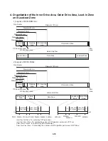


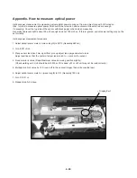

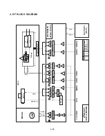

4-39
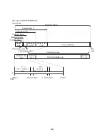
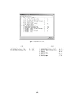
Inner Disc Test Zone : fo r performing OPC procedures.
Inner Disc Count Zone : For counting the nu mber of OPC algorithm performed in IDT Zone.
Outer Disc Test Zone :
for performing OPC procedures.
Outer Disc Count Zone :
For counting t he number of OPC algorithm perf ormed in IDT Zone.
2) Layout of DVD+R disc
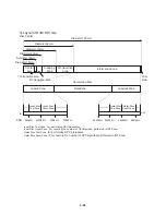
1) Layout of DVD-ROM disc
Inform ation Zone
Center
hole
Clamping
Zone
Diameter 120 mm
Diameter 15mm
Data Zone
Lead-in Zone
Lead-out Zone
Read Only Disc
Disc Center
Diameter 16mm
Diameter 22mm
3th tra nsition
area
Diameter 33mm
Diameter 44mm
1th tra nsition area
2th transition area
Rim
area
Data Zone
Lead-in
Zone
In ner Drive
Area
Unrecorded Disc
Outer Drive
Area
Inner Disc
Test Zone
in
27080H
28480H
Inform ation Zone
Center
hole
Clamping
Zone
Diameter 120 mm
Diameter 15mm
Disc Center
Diameter 16mm
Diameter 22mm
3th tra nsition
area
Diameter 33mm
Diameter 44mm
1th tra nsition area
2th transition area
Rim
area
Lead-out
Zone
23080H
PSN :
Inner Disc
Count Zone
27480H
2A480H 30000H
out
Outer Disc
Test Zone
261940H
263940H
260540H
Outer Disc
Count Zone
262940H
267940H
4. Organization of the Inner Drive Area, Outer Drive Area, Lead-in Zone
and Lead-out Zone
Summary of Contents for LRM-519
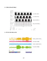
Page 30: ...3 16 WAVEFORMS 1 SYSTEM PART 1 ...
Page 31: ...3 17 2 SYSTEM PART 2 ...
Page 32: ...3 18 3 VIDEO PART 1 ...
Page 33: ...3 19 4 VIDEO PART 2 ...
Page 34: ...3 20 5 VIDEO PART 3 ...
Page 35: ...3 21 6 VIDEO PART 4 ...
Page 36: ...3 22 AI_DATA AI_CLK AI_LRCLK 7 AUDIO PART 1 ...
Page 37: ...3 23 AUD_LINK_BCLK AUD_LINK_SDIN AUD_LINK_SYNC AUD_LINK_RST 8 AUDIO PART 2 ...
Page 38: ...SPDIF 3 24 AUDIO_L 9 AUDIO PART 3 ...
Page 39: ...3 25 TXD TXD RXIN RXIN 25MHZ 10 ETHERNET PART ...
Page 40: ...3 26 FLD_RXD FLD_CLK CLK_LPC_33MHZ 11 SUPER IO FRONT INTERFACE PART ...
Page 43: ...3 29 3 POWER BLOCK DIAGRAM ...
Page 45: ...3 31 5 BLOCK DIAGRAM ...
Page 46: ......
Page 48: ...3 34 3 35 2 POWER CIRCUIT DIAGRAM A B C D E F G H I J K L M N O P Q R S T ...
Page 49: ...3 36 3 37 3 CPU CIRCUIT DIAGRAM A B C D E F G H I J K L M N O P Q R S T ...
Page 50: ...3 38 3 39 4 GMCH CIRCUIT DIAGRAM A B C D E F G H I J K L M N O P Q R S T ...
Page 51: ...3 40 3 41 5 ICH4 CIRCUIT DIAGRAM A B C D E F G H I J K L M N O P Q R S T ...
Page 52: ...3 42 3 43 6 CLOCK LPC CIRCUIT DIAGRAM A B C D E F G H I J K L M N O P Q R S T ...
Page 53: ...3 44 3 45 7 MEMORY IDE CIRCUIT DIAGRAM A B C D E F G H I J K L M N O P Q R S T ...
Page 54: ...8 LAN USB MODEM CIRCUIT DIAGRAM A B C D E F G H I J K L M N O P Q R S T 3 46 3 47 ...
Page 57: ...3 52 3 53 11 TUNER EXTERNAL AV INPUT CIRCUIT DIAGRAM A B C D E F G H I J K L M N O P Q R S T ...
Page 59: ...3 56 3 57 13 MISCELLANEDUS CIRCUIT DIAGRAM A B C D E F G H I J K L M N O P Q R S T ...
Page 60: ...3 58 3 59 14 EXTERNAL I F CIRCUIT DIAGRAM A B C D E F G H I J K L M N O P Q R S T ...
Page 61: ...3 60 3 61 PRINTED CIRCUIT DIAGRAMS 1 MAIN PRINTED CIRCUIT DIAGRAMS TOP VIEW ...
Page 62: ...3 62 3 63 2 MAIN PRINTED CIRCUIT DIAGRAMS BOTTOM VIEW ...
Page 64: ...3 66 3 67 5 POWER PRINTED CIRCUIT DIAGRAM ...
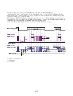
Page 84: ...4 20 9 LASER TURN ON SIGNAL F LIC502 PIN 52 LDEN DVD LCN201 PIN17 VRDC LCN201PIN 34 ...
Page 99: ...4 35 2 Disc Specification 3 Disc Materials 1 DVD ROM Single Layer Dual Layer ...
Page 119: ...4 55 4 56 CIRCUIT DIAGRAMS 1 RF CIRCUIT DIAGRAM A B C D E F G H I J K L M N O P Q R S T ...
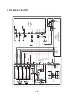
Page 120: ...4 57 4 58 2 DSP CIRCUIT DIAGRAM A B C D E F G H I J K L M N O P Q R S T ...
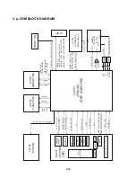
Page 121: ...4 59 4 60 3 µ COM CIRCUIT DIAGRAM A B C D E F G H I J K L M N O P Q R S T ...
Page 123: ...4 63 4 64 PRINTED CIRCUIT DIAGRAMS 1 MAIN P C BOARD LOCATION GUIDE ...


