background image

- 1-5 -

Copyright © 2007 LG Electronics. Inc. All right reserved.
Only for training and service purposes

LGE Internal Use Only

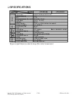
SPECIFICATIONS

[General]

[CD]

[T

uner]

AM

FM

(MW)

[T

APE

]

Power supply

Refer to the back panel of the unit.

Power consumption

10W

Mass  

kg

External dimensions (W x H x D)

300 x 252 x 171 mm

Output Power 

1W X 2     

T.H.D 10%

Speakers

8

X 2

Battery Operation

DC 9V, six "C"(R14) batteries (not supplied)

Frequency response 

100 - 18000 Hz

Signal-to-noise ratio 

55 dB 

T.H.D %
Tuning Range

87.5 -108 MHz

87.5 -108 MHz/65 -108 MHz 

Intermediate Frequency

10.7 MHz

Antenna

Telescopic antenna

Tuning Range

522-1620KHz or 530-1720KHz

Intermediate Frequency

455 kHz

Antenna

Ferrite bar antenna

Recording System

4 Tracks 2 channel stereo

Frequency Response

125 - 8000Hz

Signal to Noise Ratio

35/40dB (REC/PLAY)

Designs and specifications are subject to change without notice for improvement.

LPC-M140A

MODEL

SECTION

LPC-M140X

0.5 

3.0

Summary of Contents for LPC-M140X

Page 1: ...08F OCTOBER 2007 PORTABLE CD CASSETTE RECORDER SERVICE MANUAL MODEL LPC M140A X Website http biz lgservice com Internal Use Only This S M developed for the SVC of the unit which is indicated with the SVC Model No LPC M140N in the Main Label NOTICE ...

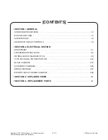
Page 2: ...1 2 ESD PRECAUTIONS 1 4 SPECIFICATION 1 5 IDENTIFICATIONS OFCONTROLS 1 6 SECTION 2 ELECTRICAL SECTION ADJUSTMENT 2 1 TROUBLESHOOTING GUIDE 2 2 INTERAL BLOCK DIAGRAM OF ICs 2 9 IC TR VOLTAGE PIN DESCRIPTION 2 15 BLOCK DIAGRAM 2 19 SCHEMATIC DIAGRAMS 2 23 WIRING DIAGRAM 2 27 PRINTED CIRCUIT BOARD DIAGRAM 2 29 SECTION 3 EXPLODED VIEWS 3 1 SECTION 4 REPLACEMENT PARTS 4 1 ...

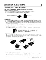
Page 3: ...stment point and installation screws should absolutely never be touched 4 Laser beams may damage the eyes Absolutely never permit laser beams to enter the eyes Also NEVER switch ON the power to the laser output part lens etc of the pick up if it is damaged 5 Cleaning the lens surface If there is dust on the lens surface the dust should be cleaned away by using an air bush such as used for camera l...

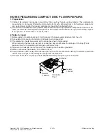
Page 4: ...where there is excessive dust 2 Notes for repair 1 Before replacing a component part first disconnect the power supply lead wire from the unit 2 All equipment measuring instruments and tools must be grounded 3 The workbench should be covered with a conductive sheet and grounded When removing the laser pick up from its conductive bag do not place the pick up on the bag This is because there is the ...

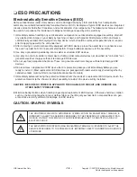
Page 5: ...s not classified as anti static can generate electrical charges sufficient to damage ESD devices 5 Do not use freon propelled chemicals These can generate electrical charges sufficient to damage ESD devices 6 Do not remove a replacement ESD device from its protective package until immediately before you are ready to install it Most replacement ESD devices are packaged with leads electrically short...

Page 6: ...ation DC 9V six C R14 batteries not supplied Frequency response 100 18000 Hz Signal to noise ratio 55 dB T H D Tuning Range 87 5 108 MHz 87 5 108 MHz 65 108 MHz Intermediate Frequency 10 7 MHz Antenna Telescopic antenna Tuning Range 522 1620KHz or 530 1720KHz Intermediate Frequency 455 kHz Antenna Ferrite bar antenna Recording System 4 Tracks 2 channel stereo Frequency Response 125 8000Hz Signal t...

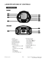
Page 7: ...AM TAPE 3 VOLUME CONTROL DIAL 4 DISPLAY WINDOW indicator 5 LEFT RIGHT SPEAKER 6 TAPE DOOR 7 CD FUNCTION buttons CD BACKWARD SKIP SEARCH button 10 BUTTON CD FORWARD SKIP SEARCH button CD REPEAT button CD STOP button CD PLAY PAUSE button 8 TAPE FUNCTION buttons TAPE PAUSE II button TAPE STOP EJECT button FAST FORWARD button REWIND button TAPE PLAY button RECORD button 9 CD DOOR OPEN OPEN button 10 S...

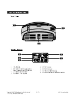
Page 8: ...ernal Use Only Rear Panel Display Window 1 2 3 4 5 6 Rear Panel Display Window 1 FM ANTENNA 2 RIF FM MODE SWITCH ST MONO HEADPHONE SOCKET 3 5mm 3 AC POWER INPUT SOCKET 4 CD REPEAT PLAY indicator 5 CD PLAY indicator 6 CD PAUSE indicator 7 CD TRACK NUMBER indicator 8 CD SYNCHRONIZED RECORDING indicator 7 8 ...

Page 9: ... 1 8 Copyright 2007 LG Electronics Inc All right reserved Only for training and service purposes LGE Internal Use Only ...

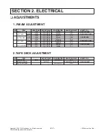
Page 10: ...t several times HI L108 IC101 PIN18 1650kHz TC3 3 AM TRACKING LOW L108 IC101 PIN18 600kHz L108 GAIN MAXIMUM HI L108 IC101 PIN18 1400kHz TC4 4 FM COVER LOW C101 IC101 PIN18 87 00MHz L104 Repeat several times HI C101 IC101 PIN18 108 5MHz TC2 5 FM TRACKING LOW C101 IC101 PIN18 90MHz L103 GAIN MAXIMUM HI C101 IC101 PIN18 106MHz TC1 2 TAPE DECK ADJUSTMENT NO ITEM OUTPUT POINT SPECIFICATION ADJUSTING PO...

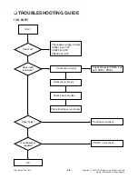
Page 11: ...Start Power on Check disc circuitry Check connector PN400 402 403 CN401 PN404 Check laser circuitry Check Focus circuitry Check tracking servo circuitry Tracking servo check PN702 1 4pin check Check power supply circuitry IC403 1 4pin 7 2V IC403 2pin 3 3V PN402 4pin 3 3V Does initial read work Does it play OK Is audio output supplied CD PART ...

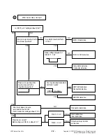
Page 12: ...s IC400 pin38 voltage transmitted Check the change of SL SL Voltage IC402 pin 17 18 DoesPN404pin2voltagechange whenopen close CN401connectordefective IC400 Defective IC402 Defective PICK UP defective Does laser light focus coil drive wareform TRACKING ERROR wareform Is rotation normal IC401 defective PICK UP defective Is HF signal normal without dropout Is FA waveform output at IC402 pin3 Is TE wa...

Page 13: ...orm IC140 Does voltage appear at IC402 17 18 MCU IC defective MICOM defective Connector defective IC400 402 Defective Slide motor defective Connector defective LMT SW defective Connector defective Q400 defective laser defective Defective laser and or connector Has pick up returned to the innermost position Does pick up stop after naving moved to the innermost position Are input output detected at ...

Page 14: ... YES YES YES YES Whe laser light Does lenses move up and down Is signal output at focus search ferminal Is signal output at PN400 pin13 16 Is IC401 pin15 FEO signal output Is IC401 pin8 SEL signal output IC401 defective IC402 defective Autuator short Connecter short Connecter short IC401 defective Laser diode degraded Pick up defective ...

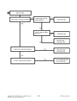
Page 15: ...01 pin1 12 Replace diode Fuse change Is B applied to pn701 No No Yes SW 702 check Yes Transformer check Yes Is Q703 704 normal Fuse open No Replace Q703 704 No D901 904 normal Tuner Abnormal Q901 ZD901 check Does 4 5V come out at IC101 pin6 No SW 702 check Yes Q101 102 check IC101 check Yes Does signal come out at pin13 14 No Is B applied to Q102 No 1 2 Tuner ...

Page 16: ...come out from speaker Yes CN202 check SW201 check HEAD connector check Yes Does signal come out at IC202 pin4 11 No Does B come out at Q901 collection No CN202 check No TAPE REC ABNORMAL HEAD connector check CN202 pin3 4 check Does IC201 pin4 11 signal come out No Does B light at leaf switch No Yes R203 L204 L203 check Does departure signal go into pn201 pin1 3 No Does L203 depart Yes Yes Yes 1 4 ...

Page 17: ... light Check LCD supply power in the power circuitry Is MICOM reset circuit normal No Supply circuitry defective Check pn403 pin4 No Supply circuitry defective MICOM surrounding circuit defective No X400 defective No Pattern defective LCD light defective 0V VDD Reset 3 3V 3 3V 0V Yes Is MICOM IC400 pin41 42 normal osc 0 125usec Yes MICOM IC400 pin52 53 54 55 output wareform normal Yes 3 3V ...

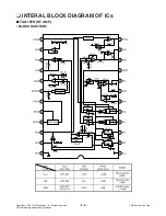
Page 18: ... 2 9 Copyright 2007 LG Electronics Inc All right reserved Only for training and service purposes LGE Internal Use Only INTERAL BLOCK DIAGRAM OF ICs TA2175FN RF AMP BLOCK DIAGRAM ...

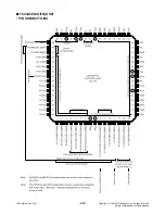
Page 19: ... 2 10 Copyright 2007 LG Electronics Inc All right reserved Only for training and service purposes LGE Internal Use Only TC94A58FAG FB DSP PIN CONNECTOINS ...

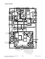
Page 20: ... 2 11 Copyright 2007 LG Electronics Inc All right reserved Only for training and service purposes LGE Internal Use Only BLOCK DIAGRAM ...

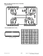
Page 21: ... 19 18 17 16 15 8 9 10 11 12 13 14 HSOP 26D TOP VIEW 1 2 3 4 5 6 7 8 9 10 11 12 13 14 15 16 17 18 19 20 21 22 23 24 25 26 27 28 ch1 OUT ch3 OUT ch4 OUT ch4 OUT ch3 OUT ch1 OUT SubGND SubGND ch2 OUT ch2 OUT ch1 IN ch3 IN ch4 IN Bias ch2 IN NC NC NC NC NC Vcc Vcc GND NC NC NC REG OUT Tr B MM1669XP MOTOR DRIVE FOR CD PLAYERS BLOCK DIAGRAM PIN ASSIGNMENTS TOP VIEW ...

Page 22: ... 2 13 Copyright 2007 LG Electronics Inc All right reserved Only for training and service purposes LGE Internal Use Only TA2111N AM FM BLOCK DIAGRAM UTCA8227P POWER BLOCK DIAGRAM ...

Page 23: ... 2 14 Copyright 2007 LG Electronics Inc All right reserved Only for training and service purposes LGE Internal Use Only AN7312 PLAY REC BLOCK DIAGRAM ...

Page 24: ...0 B S B S 2 10 0V 11 OUT OUT 2 5 8V 12 VCC Vcc 1 11 0V POWER PART 1 UTC8227P PIN NO SYMBOL DESCRIPTION VOLT V I O 1 S 10 I O port 5 LCD segment output CD processor function 0V 2 S 11 I O port 5 LCD segment output CD processor function 3 2V 3 S 12 I O port 5 LCD segment output CD processor function 0V 4 AD 1 I O port 6 LCD segment output CD processor function 0V 5 AD 2 I O port 6 LCD segment output...

Page 25: ... pin 1 6V I 5 TNI Sub beam amp input pin 1 6V I 6 Monitor photo diode amp input pin 0 5V I 7 LDO Lasser diode amp output pin 2 6V O 8 SEL APC circuit ON OFF control signal 0V I 9 TEBC Tracking error balance adjustment signal input pin 1 6V I 10 TEN Tracking error signal generation amp negative phase 1 6V I 11 TEO Tracking error signal generation amp output pin 1 6V O 12 RFDC RF signal peak detecti...

Page 26: ...LGE Internal Use Only Copyright 2007 LG Electronics Inc All right reserved Only for training and service purposes 2 19 2 20 BLOCK DIAGRAM LPC M140A AX ...

Page 27: ...Copyright 2007 LG Electronics Inc All right reserved Only for training and service purposes LGE Internal Use Only 2 21 2 22 BLOCK DIAGRAM LPC M140A D ...

Page 28: ...Copyright 2007 LG Electronics Inc All right reserved Only for training and service purposes 2 23 2 24 SCHEMATIC DIAGRAMS 1 MAIN SCHEMATIC DIAGRAM 2007 06 29 A 1 2 3 4 5 6 7 8 9 10 11 12 B C D E F G H I J K L M N O P Q R S T ...

Page 29: ...007 LG Electronics Inc All right reserved Only for training and service purposes LGE Internal Use Only 2 25 2 26 2 MP3 SCHEMATIC DIAGRAM 2007 06 29 A 1 2 3 4 5 6 7 8 9 10 11 12 B C D E F G H I J K L M N O P Q R S ...

Page 30: ...LGE Internal Use Only Copyright 2007 LG Electronics Inc All right reserved Only for training and service purposes 2 27 2 28 WIRING DIAGRAM ...

Page 31: ...Copyright 2007 LG Electronics Inc All right reserved Only for training and service purposes LGE Internal Use Only 2 29 2 30 PRINTED CIRCUIT DIAGRAM 1 MAIN P C BOARD DIAGRAM 2 POWER P C BOARD DIAGRAM ...

Page 32: ... 456 457 A49 266 265 250 455 267 A42 457 253 456 252 456 LEAF SW 251 289 452 457 457 260 261 292 273 298 459 458 288 295 293 301 273 300 303 302 459 459 292 A45 452 282 277 286 263 263 S E T O N N A N I H T I W T N I O P N O I T A M A L C X E E H T D E D N E T N I S I E L G N A I R T L A R E T A L I U Q E L E N N O S R E P E C I V R E S E H T T R E L A O T T N A T R O P M I F O E C N E S E R P E H...

Page 33: ...Copyright 2007 LG Electronics Inc All right reserved Only for training and service purposes LGE Internal Use Only 3 3 3 3 ...

Reviews: