background image

2-39

2-40

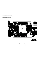
• MAIN P.C. BOARD DIAGRAM 

Summary of Contents for LAC-M7600

Page 1: ... MP3 WMA Receiver SERVICE MANUAL CAUTION BEFORE SERVICING THE UNIT READ THE SAFETY PRECAUTIONS IN THIS MANUAL P N AFN30086098 APRIL 2006 MODELS LAC M7600R LAC M7600 SERVICE MANUAL MODELS LAC M7600R LAC M7600R ...

Page 2: ...ELECTRICAL ELECTRICAL TROUBLESHOOTING GUIDE 2 1 WAVEFORMS OF MAJOR CHECK POINT 2 6 INTERNAL BLOCK DIAGRAM of ICs 2 7 BLOCK DIAGRAM 2 21 SCHEMATIC DIAGRAMS 2 23 PRINTED CIRCUIT DIARGAMS 2 31 SECTION 3 EXPLODED VIEWS CABINET AND MAIN FRAME SECTION 3 1 MECHANISM PICK UP 3 3 SECTION 4 REPLACEMENT PARTS LIST 4 1 ...

Page 3: ...t instrument positive lead Always remove the test instrument ground lead last 1 The service precautions are indicated or printed on the cabinet chassis or components When servicing follow the printed or indicated service precautions and service materials 2 The Components used in the unit have a specified conflammability and dielectric strength When replac ing any components use components which ha...

Page 4: ...harges sufficient to damage ESD devices 5 Do not use freon propelled chemicals These can generate electrical charges sufficient to damage ESD devices 6 Do not remove a replacement ESD device from its protective package until immediately before you are ready to install it Most replacement ESD devices are packaged with leads electrically shorted together by conductive foam aluminum foil or comparabl...

Page 5: ... that permission is required in order to download MP3 WMA files and music from the Internet Our company has no right to grant such permission Permission should always be sought from the copyright owner 1 GENERAL Output Power 50W x 4CH Max Power Source DC 12V Speaker impedance 4 8 Ω Ground System Negative Dimensions W x H x D 182 x 51 x 173 mm Without Front Panel Net Weight 1 3 kg 2 CD Frequency Re...

Page 6: ...reading occur Can disc be played Is audio output supplied OK Check audio circuitry IC506 IC508 PN502 Check tracking servo circuitry Q501 IC506 IC504 Check DISC Check focusing circuitry Q501 IC506 Check laser circuitry Q501 IC506 Check loading supply circuitry Q701 Q702 Q703 Q704 PN503 Q503 IC508 Check power supply circuitry Q722 Q727 IC702 Q723 Q805 Q806 Q720 Q719 IC701 ...

Page 7: ...4 defective X101 X102 C101 C102 C103 C104 PN103 PN802 PN901 CN903 front PCB pattern defective IC102 Pin75 76 78 front PCB pattern defective VFD901 D908 Surrounding circuit defective Display LCD connector defective Is VFD901 F Pin1 2 F Pin40 41 Differential Voltage 2 1 3 15V Input Is u com IC102 Pin75 76 78 output waveform normal Is u com IC102 reset circuit normal IC102 74Pin Is u com IC102 keyin ...

Page 8: ... 72 70 DSP WAVEFORM 5 Check the Data transmission from Pin21 to MICOM WAVEFORM 5 IC510 Check the TRVP Voltage IC506 Pin23 Check the change of SL SL Voltage IC504 Pin13 14 Does FA waveform appear at IC506 Pin23 WAVEFORM 3 Laser light check A focus coil drive wareform TRACKING ERROR wareform Defective contact PN501 Defective PICK UP Defective IC504 Defective IC506 Defective IC504 Defective MICOM Def...

Page 9: ...tput from LMT SW applied to 68 of IC510 Is data transferred from IC510 Does voltage appear at IC504 Pin 13 14 Defective MICOM IC510 Defective IC506 Defective slide motor and or connector PN504 Defective LMT SW and or connector PN504 Defective MICOM IC510 Defective IC506 Is power supplied to laser Q501 Q501 collector about 1 8V OV YES YES YES YES YES YES NO NO NO NO NO NO OPEN CLOSE ...

Page 10: ...06 Pin25 WAVEFORM 3 Check the signal of IC504 Pin 15 16 WAVEFORM 3 Defective IC506 Defective IC506 Degraded laser diode Defective PICK UP Defective IC506 Defective IC504 Defective contact PN501 or Defective PICK UP Check the change for SP SP Voltage of IC504 Pin11 12 WAVEFORM 1 Check the change for SPDO Voltage of IC506 Pin21 WAVEFORM 1 ...

Page 11: ...during TOC reading 2 RF WAVEFORM IC506 45 IC506 49 during TOC reading 4 TRACK DRIVE AND MOTOR WAVEFORM IC502 24 IC504 17 during TOC reading 3 FOCUS DRIVE AND MOTOR WAVEFORM IC506 25 IC504 15 When focus search failed or there is no disc on tray There is disc on tray and focus search success ...

Page 12: ... 2 7 INTERNAL BLOCK DIAGRAM of ICs FRONT 1 MICOM PIN Assignment ...

Page 13: ... 2 8 2 Pin Descriptions ...

Page 14: ... 2 9 ...

Page 15: ... 2 10 3 Pin Descriptions ...

Page 16: ...7 18 19 21 24 23 12 15 14 1 20 6 RL IN1 IN2 IN3 IN4 13 C1 C1 C1 C1 PRE GND 10 25 22 OUT1 PW GND1 OUT1 OUT2 PW GND2 OUT2 OUT3 PW GND3 OUT3 OUT4 PW GND4 OUT4 TAB VCC1 VCC2 C 3 C 4 C 2 PRE GND PW GND STBY RIP MUTE C 5 16 C6 4 Off set DET MUTE PLAY 5 V R1 AC GND ...

Page 17: ... 2 12 78K0 KF2 1 Block Diagram ...

Page 18: ...NI5 P26 ANI6 P27 ANI7 P60 CSL0 P61 SDA0 P62 EXSCL0 P63 P33 TI51 TO51 INTP4 P64 P65 P66 P67 P77 KR7 P76 KR6 P75 KR5 P74 KR4 P73 KR3 P72 KR2 P71 KR1 P70 KR0 P06 TI011 T001 P05 TI001 SSI11 P32 INTP3 P120 INTPO EXLVI P47 P46 P45 P44 P43 P42 P41 P40 RESET P124 XT2 EXCLKS P123 XT1 IC FLMD0 P122 X2 EXCLK P121 X1 REGC VSS EVSS VDD EVDD 80pin QFP 1 2 3 4 5 6 7 8 9 10 11 12 13 14 15 16 17 18 19 20 60 59 58 ...

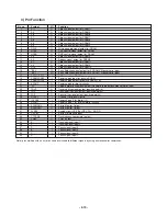
Page 19: ... 2 14 3 Pin Function ...

Page 20: ... 2 15 AM5810 1 Block Diagram ...

Page 21: ... 2 16 3 Pin Function ...

Page 22: ... PRAMVDD15 PRAMVDD33 SPOUT PC TRWP TRP FOP PMCK SMCK DOSYTXT MRST BLKCK STAT MLD MDATA MCLK TX FLAG EXT2 EXT1 EXT0 MSRVWOMON DVSS3 OUTR AWDD1 AWSS1 OUOTL PLLFO PLLF IREF DSLF ARFIN 50 49 48 47 46 45 44 43 42 41 40 39 38 37 36 35 34 33 32 31 30 29 28 27 26 76 77 78 79 80 81 82 83 84 85 86 87 88 89 90 91 92 93 94 95 96 97 98 99 100 MN6627954 75 74 73 72 71 70 69 68 67 66 65 64 63 62 61 60 59 58 57 5...

Page 23: ... DSL PLL VCO DSLPLL SPINDLE SERVO SPD SERVO CPU DSV MP3 WMA DECORDER ANALOG LOWPASS FILTER DIGITAL FILTER 1bit DAC PWM LOGIC DF MASH SERIAL OUTPUT INTERFACE DAO BUS CONTROL UNIT BCU CIRC RAM 1Mbit DRAM SUBCODE INTERFACE DEMECC TXTCK PLLFO IOVDD1 IOVDD2 DRVDD DVDD1 DVDD2 DVSS1 DVSS2 DVSS3 OUTL OUTR AVDD1 AVSS1 TX LRCKIN BCLKIN SRDATIN PLLF DSLF IREF ARFIN MDATA MCLK MLD STAT PMCK SMCK X2 X1 TXTD DQ...

Page 24: ...9 PRAMVDD33 I Power supply input for built in DRAM 20 PRAMVDD15 Power supply output for built in DRAM 1 6V 21 SPOUT O Power supply for digital circuits 22 PC I O Spindle motor drive signal output Absolute value output Monitor serial input 23 TRVP O Traverse drive signal output positive polarity 24 TRP O Tracking drive signal output positive polarity 25 FOP O Focus drive signal output positive pola...

Page 25: ... 31 29 30 N C N C AUXR PDL PD N C PDR MIX N C GND N C A D S L C S N I A S E T U M T U O A S W S T U O R O L I F 3 T U O 2 C A R N I 2 C A R R T U O F R U O C N R T U O C A W S N I C A W S T U O C A f e r C C N L M A R M A L D M R D M L X U A N C OUTLR OUTLF FILOL AC2OUTL AC2INL VDD VREFOUT ACINL ACOUTL ACINR TQFP44 12 13 14 15 16 ...

Page 26: ... BLOCK DIAGRAM 2 21 2 22 ...

Page 27: ...2 23 2 24 SCHEMATIC DIAGRAMS MAIN SCHEMATIC DIAGRAM ...

Page 28: ...2 25 2 26 MAIN 2 SCHEMATIC DIAGRAM ...

Page 29: ...2 27 2 28 MAIN 3 SCHEMATIC DIAGRAM ...

Page 30: ...2 29 2 30 MAIN 4 SCHEMATIC DIAGRAM ...

Page 31: ...2 31 2 32 FRONT SCHEMATIC DIAGRAM ...

Page 32: ...2 33 2 34 CD SCHEMATIC DIAGRAM ...

Page 33: ...2 35 2 36 TRIM SCHEMATIC DIAGRAM ...

Page 34: ...2 37 2 38 PRINTED CIRCUIT BOARD DIAGRAMS MAIN P C BOARD DIAGRAM ...

Page 35: ...2 39 2 40 MAIN P C BOARD DIAGRAM ...

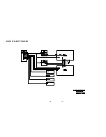
Page 36: ...2 41 2 42 FRONT TRIM P C BOARD DIAGRAM TRIM P C BOARD ...

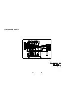
Page 37: ...2 43 2 44 CD P C BOARD ...

Page 38: ...4 451 281 276 451 275 451 450 451 451 452 456 279 451 274 273 269 266 268 264 A45 262 261 262 A50 457 263 453 260 265 272 270 271 280 278 259 252 A40 450 255 256 257 258 253 450 251 A42 250 SECTION 3 EXPLODED VIEWS CABINET AND MAIN FRAME SECTION ...

Page 39: ...3 3 3 4 2 3 4 5 1 1 2 A03 MECHANISM PICK UP ...

Reviews: