COLOR MONITOR
SERVICE MANUAL
CAUTION
BEFORE SERVICING THE UNIT,
READ THE SAFETY PRECAUTIONS IN THIS MANUAL.
CHASSIS NO. : LM72A
MODEL:
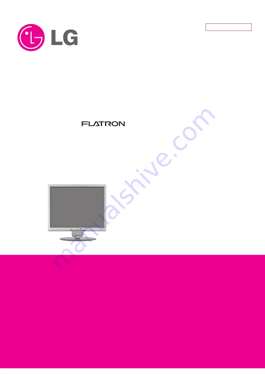
L1942H
E
(L1942H
E
-BFT.A***
O
PN)
*To apply the MSTAR Chip .
(
) **Same model for Service
Website:http://biz.LGservice.com
Internal Use Only
AUTO/SET
VOLUME


