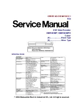
background image

Super Multi DVD Drive

S E RVICE MANUAL

MODEL: GSA-4165B/

G S A - 4 1 6 7 B /
G S A - 4 1 6 8 B

P/NO : 3828HS1047G

August 2005

Printed in Korea

MODEL : GSA-4165B/GSA-4167B/GSA-4168B

Summary of Contents for GSA-4165B

Page 1: ...SuperMultiDVDDrive SERVICE MANUAL MODEL GSA 4165B GSA 4167B GSA 4168B P NO 3828HS1047G August 2005 Printed in Korea MODEL GSA 4165B GSA 4167B GSA 4168B ...

Page 2: ...ation 28 3 Disc Materials 28 4 Writing Pulse Waveform of DVD R 31 5 Writing Pulse Waveform DVD RW 33 6 Organization of Inner Drive Area Outer Drive Area Lead in Zone and Lead out Zone 34 LightScribe MEDIA 36 39 1 LightScribe Media 36 2 Hardware Block Diagram of LightScribe Label Printing 37 3 MD Assy For LightScribe 38 4 Optical Encoder Assy 39 DVD CD DATA PROCESSING 40 43 1 Data Processing Flow 4...

Page 3: ... read only 16x write 16x write DVD RW 4x or 6x write 4x or 6x write 4x or 6x write read only 4x or 6x write 4x or 6x write DVD R DL 4x write 4x write 4x write read only 4x write 4x write DVD R 16x write read only 16x write 16x write read only read only DVD RW 8x write read only 8x write 8x write read only read only DVD R DL 4x or 6x write read only 4x or 6x write 4x or 6x write read only read only...

Page 4: ... R DL Double Layer and DVD RW 3 Reads data in each CD ROM CD ROM XA CD I Video CD CD Extra and CD Text 4 Reads data in Photo CD Single and Multi session 5 Reads standard CD DA 6 Support to read Super Audio CD Compatible layer in Hybrid type 7 Reads and writes CD R discs conforming to Orange Book Part 2 8 Reads and writes CD RW discs conforming to Orange Book Part 3 9 Reads DVD RAM with CPRM and DV...

Page 5: ...x DVD R DL 8x max DVD RAM Ver 1 0 2 2 2x 2x 3x ZCLV 3x 5x PCAV DVD Video CSS Compliant Disc 8x max Single Dual layer DVD R RW 10x 8x max DVD R DL 8x max CD R RW ROM 48x 40x 48x max CD DA DAE 40x max 80mm CD 16x max 4 Sustained Transfer rate DVD ROM 22 16 Mbytes s 16x max CD ROM 7 200 kB s 48x max 5 Burst Transfer rate Ultra DMA Mode2 Multi word DMA Mode2 PIO Mode 4 6 Multimedia MPC 3 compliant 5 A...

Page 6: ...D Multi Session Video CD CD Audio Disc Mixed mode CD ROM disc data and audio CD Extra CD Text CD R Conforming to Orange Book Part2 read write CD RW Conforming to Orange Book Part3 read write 2 2 Writing method 1 DVD R RW Disc at Once Incremental Recording Restricted Overwrite DVD RW only 2 DVD R DL Disc at Once Incremental Recording Layer jump Recording 3 DVD RAM RW Random Write 4 DVD R Sequential...

Page 7: ...OM Single layer 6 7x 16x CAV Approx 9 420 r min Dual layer 5 0x 12x CAV Approx 7 770 r min DVD R DL 8 5GB 3 3x 8x CAV Approx 5 180r min DVD Video CSS 3 3x 8x CAV Approx 5 180 r min DVD R 4 7GB 4 2x 10x CAV Approx 5 890 r min DVD RW 4 7GB 3 3x 8x CAV Approx 4 720 r min DVD RAM Ver 1 0 2 2 2x 2x 3x ZCLV 3x 5x PCAV DVD R 4 7GB 4 2x 10x CAV Approx 5 890 r min DVD R DL 8 5GB 3 3x 8x CAV Approx 5 180 r ...

Page 8: ...W 4 58 11 08 Mbytes s 8x max DVD RAM Ver 1 0 2 77 Mbytes s 2x ZCLV Ver 2 2 2 77 4 155 4 155 6 93 Mbytes s 2x 3x ZCLV 3 5x PCAV DVD R 5 73 13 85 Mbytes s 10x max DVD R DL 4 58 11 08 Mbytes s 8x max DVD RW 4 58 11 08 Mbytes s 8x max CD R ROM 3 000 7 200 kB s 48x max CD RW 2 500 6 000 kB s 40x max CD DA DAE 2 500 6 000 kB s 40x max 3 3 2 Burst transfer rate Ultra DMA Mode 2 33 3 Mbytes s max Multiwor...

Page 9: ...5V DC 1 3A typ 1 5 A max 12V DC 0 9A typ 1 5 A max Read Active 5V DC 1 0A typ 1 5 A max 12V DC 0 9A typ 1 5 A max Seek Acess 5V DC 1 0A typ 1 5 A max 12V DC 1 2A typ 2 0 A max 5 3 Standby Sleep mode No disc 1 1 W typ 1 3 W max 6 AUDIO PERFORMANCE Output Level 1kHz 0dB 0 7 Vrms typical Frequency Response 3dB 20 to 20 000Hz Signal to Noise Ratio 80 dB min with IHF A and LPF 20 kHz THD 1kHz 0dB 0 10 ...

Page 10: ...ht cause damage to the loading section of the drive 2 Stop Eject button This button is pressed to open the CD tray This button works only when power is supplied to the drive 3 Emergency Eject Hole Insert a paper clip here to eject the Disc tray manually or when there is no power 4 Drive activity indicator Two colored LED is used to indicate the operation of the Drive Drive Activity Indicators Stop...

Page 11: ...se a short circuit and damage the system Always turn the power OFF when connecting or disconnecting the cable 3 Jumper Connector This jumper determines whether the drive is configured as a master or slave Changing the master slave configuration takes effect after power on reset 4 Analog Audio Output Connector Provides output to a sound card analog signal Generally you need this to play a regular a...

Page 12: ... in the direction of arrow 4 See Fig 1 3 B When the CD tray has been opened completely lift 2 points a and remove the CD tray while drawing out simultaneously C Remove the Soldering of the LD and LD b for the Loading Motor and then remove the Main Circuit Board D At this time be careful not to damage the 4 connectors of the Main Circuit Board 2 MECHANISM ASSY DISASSEMBLY 2 1 Pick up Unit A Release...

Page 13: ...2 2 Pick up A Release 1 screw C and remove the Pick up Pick up Unit Pick up C Fig 2 2 13 ...

Page 14: ...020 021 050 430 005 035 004 006 A B C D E F G H 1 2 3 4 5 452 024 481 034 027 026 033 025 430 445 020 453 031 036 453 010 011 009 008 012 016 015 013 PBM00 MAIN C B A PBF00 FRONT C B A 482 482 482 001 482 003 002 LightScribe only 14 15 EXPLODED VIEW ...

Page 15: ...hanged conditions of disc and change in operating temperature Jitter The 16 value of the time variation between leading and trailing edges of a specific I3 I11 pit or land as measured by Time Interval Analysis Deviation The difference between a fixed value of Pit length and Land length TOC Table Of Contents in the Lead in Area the subcode Q channel contains information about the Tracks on the disc...

Page 16: ...pitch p Radial Direction Iw A O a a Groove Land Radial Error Signal The Groove wobble Average center Actual center CD ROM READ ONLY DISC a 30nm ITEM CD ROM CD R CD RW Standard Yellow Book Orange Book II Orange Book III Record Not available Write once Re Writeable Tracking Signal I11 Itop 0 6 0 6 0 55 M11 0 70 HF Modulation Read Laser Power mW 0 5 mW 0 7 mW 1 0 mW Jitter 35 nsec 35 nsec 35 nsec Ref...

Page 17: ...t and Land on the disc It is so called WORM Write Once Read Many CD It is composed of polycarbonate layer Organic dye layer Reflective layer and Protective layer Gold Silver Reflective layer is used to enhance the reflectivity According to the kinds of Organic dye layer it is divided by Green CD Gold CD Blue CD Laser Wavelength 780 nm Laser Power read 0 7 mW Recording Power 8x 14 20mW 16x 25 35mW ...

Page 18: ... reading is enabled by the difference of reflectivity It is possible to overwrite about 1000 times Laser Wavelength 780 nm Laser Power Read 1 0mW Recording Power Erase 4 18mW Write 6 45mW When disc rewriting new data is overwritten previously recorded data Polycarbonate layer has a Pre Groove which make a track Lens H D Beam Spot Focusing Lens Laser Spot at Constant Read Intensity Reflected Light ...

Page 19: ...Spot Recorded Mark Reflected Light Signal Reflected Light Signal Below ORP Mark Too Short At Optimum Record Power ORP Above ORP Mark Too Long Time 6 Writing process of CD RW Disc Write Power Erase Power Read Power Groove Crystal Amorphous Amorphous Recorded state lower reflectivity Melting quenching Heating gradual cooling Crystal phase Erased state higher reflectivity ...

Page 20: ...Area Lead out Area Center hole Clamping and Label Area Information Area PCA PMA Test Area Count Area Diameter 15 mm Diameter 45 mm Diameter 120 mm Unrecorded Disc Tsl 00 35 65 Tsl 00 15 05 Tsl 00 13 25 Tsl 99 59 74 00 00 00 in out Test Area for performing OPC procedures Count Area to find the usable area immediately in T A Tsl start time of the Lead in Area as encoded in ATIP PMA Program Memory Ar...

Page 21: ...ad_In area so that general Driver can read it Because PCA and PMA area exist before Lead In area General CD Player or CD ROM Drive can t read these areas 9 OPC and ROPC 1 OPC Optimum Power Control This is the first step of writing process because CD writer has its own laser power value and media have different writing characteristics This is determined by the Writing characteristic speed temperatu...

Page 22: ...a close Reference B level value c Normalization of B level is used to eliminate the effect of reflectivity fluctuation The reflected B level value is normalized by the disc reflectivity itself CD R RW Media Write Strategy Determination PCA Test Area Program Area PMA Area Lead In Area Lead out Area OPC PCA Count Area ROPC Recording Capacity of CD R RW 74Minute Recording media 2048 Byte Sector X 75 ...

Page 23: ...27 The differences of DVD R RW DVD R RW discs and DVD ROM 1 Recording Layer LPP Land Pre Pit DVD R RW Disc DVD R RW Disc 0 74um 3T 0 4um DVD ROM Read Only Disc ...

Page 24: ...itch 0 74 0 74 0 74 0 74 0 74 0 74 Minimum pit length 0 4 0 44 0 4 0 4 0 4 0 4 Modulation 0 6 0 6 0 6 0 6 0 6 0 6 Channel bit rate 26 16MHz 26 16MHz 26 16MHz 26 16MHz 26 16MHz 26 16MHz Wobble Frequency 140KHz 140KHz 817 4KHz 817 4KHz Addressing 26 16MHz 26 16MHz Wobble LPP Wobble LPP Wobble ADIP Wobble ADIP Read Power mW 0 7 0 1 0 7 0 1 Write Power mW JItter 8 8 8 8 9 9 Bondinglayer Polycarbonate ...

Page 25: ...ing layer dye Disc substrate Adhesive layer Protective layer Reflective layer Dye layer Substrate Laser beam Disc structure Disc structure Recording Recording is done by changing the organic dye layer and the substrate with a laser when a strong is applied to a disc the temperature of the ortanic dye material goes up the dye is decomposed and the substrate changes at the same time At this time a d...

Page 26: ... Recording layer Phase change material Dielectric layer Disc substrate DVD RW Adhesive layer Protective layer Reflective layer Dielectric layer Recording layer Phase change material Dielectric layer Disc substrate Disc structure Recording principles Recording When a high power laser is applied to the recording material it melts and then becomes amorphous with a low reflection coefficient when it q...

Page 27: ...lses a blocked write strategy where each single mark is created by one continuous pulse 1 1st Method Using Pulsed Write Strategy 3T NRZI T 3 2Tw Ttop dTtop dTle Pb top top le Pp Channel bits N 3 only the top pulse T first pulse lead time dT dT NRZI T 4 2Tw Tw Ttop Tmp Tmp Tlp dTtop dTle Pb top top le lp mp Pp Channel bits N 4 the top pulse T multi pulse T and last pulse T first pulse lead time dT ...

Page 28: ...Tw 1 25Tw dTtop 4 dPp4 Ttop 4 Tlp Ttop 4 Ttop 4 Tmp Tmp Tlp Tlp Tmp N 3 T cm 3 can be optimized individually N 4 T cm 4 x N 3 T T T T P shall be 0 1mW top mp lp w w top c Pp Actual write power Pb Bias Power dPp Additional power Only be applied for the 3T and 4T marks Pc Cooling power Especially at higher recording speeds optimum cooling down of the recording layer after writing a mark may be neede...

Page 29: ...33 5 Writing Pulse Wave Form of DVD RW NRZI Channel bits 2Tw Tw Ttop dTtop Pp Pe Tmp mp T dTera Pp Actual write power Pe Erase Power Pb Bias Power Pb 0mW Tmp ...

Page 30: ...corded Disc PSN 23080H 27080H 27480H 28480H 2A480H 30000H 260540H 261940H 262940H 263940H 267940H in OUT Disc Center Rim area Center hole 1st transition area 2nd transition area Clamping Zone 3rd transtion area Information Zone Diameter 15 mm Diameter 16 mm Diameter 22 mm Diameter 33 mm Diameter 44 mm Diameter 120 mm Disc Center Rim area Inner Disc Count Zone Outer Disc Count Zone 2 Layout of DVD ...

Page 31: ...f OPC algorithm performed in IDT Zone Lead in Zone Lead out Zone Data Zone Inner Disc Test Zone Outer Disc Test Zone Unrecorded Disc PSN 2A480H 2A7C80H 2DC80H 30000H 260540H 262940H 265940H 266140H in OUT Center hole 1st transition area 2nd transition area Clamping Zone 3rd transtion area Information Zone Diameter 15 mm Diameter 16 mm Diameter 22 mm Diameter 33 mm Diameter 44 mm Diameter 120 mm Di...

Page 32: ...e Media 1 LightScribe Media Center Hole Screen Printed Imaging Layer Clear Protective Coating Reflective Thermal Layer Dye Data Layer Polycarbonate Substrate DiscOD Label Zone Control Feature Zone Clamping Logo Zone ...

Page 33: ...nalog Signal Processor MECHANISM Optical Pick up Optical Encoder Sled Track Tilt Focus RFOUT Spindle Motor Step Motor Track Actuator Tilt Actuator Focus Actuator Laser Power Reference Write Strategy Control Buffer Memory SERVO Signals RF Cell Signals Laser Power Monitor Signal Optical FG CIrcuit ...

Page 34: ...38 3 MD Assy For LightScribe Optical Encoder Unit OPU ID Movement Range L 21um ...

Page 35: ...L OR CODESTRIP FFC 3PIN SIGNAL PROCESSING CIRCUITRY R VLED VCC CH A CH B CH B GND GND Vcc OFG Encoder PCB PIN 6 VCC PIN 5 CH A PIN 4 GND PIN 3 VLED PIN 2 GND PIN 1 CH B PIN 6 VCC PIN 5 CH A PIN 4 GND PIN 3 VLED PIN 2 GND PIN 1 CH B Optical Encoder IC Schematic of Enc PCB ...

Page 36: ...lice EFM demodulator CiRC error correction Audio DAC Buffer Memory controller CSS controller Atapi interface control Data PLL Servo ADC Focus tracking control output Sled control output CAV Spindle control P up Unit HOP 7632TS IC101 RF AMP R2S35002 CD DVD IC301 R8J32007 TE CSO GEN FE GEN DRAM U COM SRAM IC302 Flash ROM ...

Page 37: ...the regional code and plays title in the case of allowed regional code only 2 Management of DVD Disc for the scrambled of data 1 DVD ROM and DVD player of host generate the KEY 1 respectively transfer to opposite part the KEY 2 is received recognizes the data transfer or not with this value and generates the bus key encoded the data 2 Encoded Disc Key and Title Key host is transfer with the bus Ke...

Page 38: ...MPEG 2 board generates the challenge key 10 Byte and transfers to drive The board and drive generate key 1 5Byte with the challenge key respectively Of course the Algorithm generating the key 1 is not known 3 Compare with the generated key 1 if it corresponds each other the first step of authentication is completed This is a course to identify the MPEG 2 board with a drive 4 The second step of aut...

Page 39: ...UM PLW PNG NZL AUS 4 The disc has the regional code of 8 bit Example The disc manufactured in the U S A has the number one Transfer to MPEG 2 board reading the regional code Receiving data from the MPEG 2 board and output through the monitor If the board is setting to the regional code 1 for the U S A Check the received regional code to number 1 all or not transfer the data to VGA card in accordan...

Page 40: ... NC BUSY SEN SDIO SCLK MON1 VSL CLK CLKB GND GND NRZB NRZ RWB VSA RSET EN AGND ISLOP IAPC Rfreq SLG 44 Tilt 43 TR 42 TR 41 AF 40 AF 39 GND FM 38 FM 37 VREF 36 SEL 35 VCC FM 34 ENA 33 IAPC 32 SLG 31 VSA5 30 VSL25 29 CLK 28 CLKB 27 GND LDD 26 NRZB 25 NRZ 24 GND LDD 23 MONITOR 22 RWB 21 SDIO 20 SCLK 19 BUSY 18 SEN 17 VSO 16 Vcc FM 15 GND OEIC TEMP 14 RF 13 RF 12 E2 F2 11 C 10 A 9 E1 F1 8 E4 F4 7 D 6 ...

Page 41: ...trol clock 21 SDIO I O Serial data for parameters and control in out 22 RWB I Write enable for NRZ laser data L write H read 23 MONITOR O Monitor output 24 GND LDD Ground connection for LD Driver IC 25 NRZ I NRZ laser data H mark L space LVDS 26 NRZB I NRZ laser data H mark L space LVDS 27 GND LDD Ground connection for LD Driver IC 28 CLKB I CLOCK for NRZ code input LVDS 29 CLK I CLOCK for NRZ cod...

Page 42: ...od A D B C k x EF1 EF4 EF2 EF3 This signal is generated in RF IC IC101 R2S35002 and controls the pick up s left and right shift to find to track on Disc 3 RF Signal A B C D This signal is converted to DATA signal in DSP IC IC301 R8J32007 46 Pick Up module Photo Diode Tracking Focusing Infrared Iaser k F H E G A D B C A D B C k F H E G Offset TE Tp Sub2 Main Tp 2 Sub1 Track Center F E D C A B H G ...

Page 43: ...WAPC buffer 2 5VREF Buffer S H B H 13 S H MU X AM P APCDAC REDA WRDA SCLK SDATA WDEN 12 9 9 8 10 28 29 126 127 CN101 IC101 R2S35002 IC301 R8J32007 BCNT 5 6 TCPH 32 134 175 R106 R105 C106 25 26 28 120 121 123 108 C105 DESCRIPTION OF CIRCUIT 1 ALPC Automatic Laser Power Control Circuit 1 1 Block Diagram ...

Page 44: ...the other one is used at writing The logical WGATE signal which is switched between reading and writing changes the two APCDAC The ALPC loop supplies same currency IAPC to Laser Diode Driver LDD during reading and writing There is another ALPC which controls Full Scale DAC FsDAC FsDAC determines scale of WDAC of Laser Diode Driver MPU monitors write power level of FMON signal and changes FsDAC dir...

Page 45: ...generates from focus error detection block in RF IC R2S35002 using Conventional Astigmatism Detection method Differential Astigmatism Detection method Focus Gain and path can be changed at the RF IC R2S35002 according to the disc and the resulting output FE R2S35002 2pin is input to DSP IC R2S35002 169pin The Focus Search operation is using FE PE Signal therefore check FE PE signals when Focusing ...

Page 46: ...ACT IC101 R2S35002 IC301 R8J32007 MPPO A D B C G HAVC LS to V14 1 173 181 L P F L P F SPPO A D B C K EF1 EF4 EF2 EF3 Sled Compensator DAC SL2 183 SL1 182 A A B B SLED MOTOR Unit CN601 TRD R330 IC601 R2S30202FP TACT TACT EN1 EN2 CTL1 CTL2 REF C604 1 65V TOIN 39 42 20 21 36 37 SL2 2 SL1 3 SL1IN SL2IN A B 8 10 A B 6 9 SL2N SL1N SL2P SL1P C336 1 65V C338 C337 R372 1 65V R374 R373 R332 R331 ...

Page 47: ...F2 EF3 A A B B SLED MOTOR Unit A B C D G HAVC LS to V14 L P F L P F 38 79 80 81 EQ MIRR DET AGC TOP HOLD 63 62 BOTTOM HOLD TE1 MIRRTOPH MIRRBOTH C128 GND MIRR VREF1 VREF1 SL2 D A C Tracking Compensator IC301 R8J32007 173 Sled Compensator A D C 149 M U X Short Seek Algorithm Loog Seek Algorithm D A C 182 181 183 TRD SL1 Track Counter and Timer R101 C101 GND MIRR TE1 TE IP2MIRR C127 GND ...

Page 48: ...nversion Digital Equalizer Block and D A Conversion in R8J32007 the output signal TRD R8J32007 181pin is input to Drive IC 39pin The drive output signal TACT TACT generated according TOIN R2S30202FP 39pin and drives tracking actuator in the P U unit 3 2 2 Sled Servo The working distance of tracking actuator is too short to cover whole disc radius Sled Servo make P U move by little and little so th...

Page 49: ...CAV DVD ROM DL 6 DVD 16x CAV DVD ROM 7 DVD 16x PCAV DVD R When drive read PRESS CD Closed Session CD R RW the spindle motor is controlled using FG CAV Spindle Servo FG signal R2S30202FP 19pin input to SFG in DSP IC R8J32007 213pin The spindle controller in DSP IC uses SFG as spindle rotation frequency feedback therefore the FG CAV Spindle Servo doesn t work well if FG generation is abnormal The sp...

Page 50: ...VD R DL 2x 4x DVD RW 1x 2x 4x 6x DVD R 2 4x 4x 8x 12x 16x PCAV DVD R DL 2 4x 4x 6x DVD RAM 2x 3x 3 5x PCAV DVD RW 2 4x 4x 8x When drive write DVD RAM R RW R RW CD R CD RW the spindle motor is controlled using Wobble CLV Spindle Servo The WOBSIG signal R2S35002 37pin input to DSP IC R8J32007 154pin The DSP Controller in R8J32007 uses WOBSIG as linear velocity feed back therefore the Wobble CLV Spin...

Page 51: ... PORT06 PORT05 PORT04 PORT03 PORT02 PORT01 PORT00 45 LO_ZB SPDSH 44 43 BLANK 42 41 40 39 GND4 38 MPDSH SPDSH 37 RFPDSH 36 WFPDSH 35 IDGATE 34 33 SPBLVL TISH2 32 LNDTRK 31 WBLSH 30 29 28 27 WOBSIG 26 RFHLD TISH1 76 77 SUMF SUMF2 5V VCC1 AGFR AGFU 78 RFIN 79 SRVREF 80 FVREFO 81 IREFT 82 VREF1 83 HAVC 84 SA 85 SB 86 SC 87 SD 88 89 3 3V VDD2 90 MA 91 MB 92 MD 93 GND2 94 AIN1 95 AIN2 96 MC 97 AIN3 98 S...

Page 52: ...LO_ZB SPDSH pin D D D D D D D D D D D A D SUBP N IP2 MIRR D SUBW BPO to MIRR DEFECT EQOP N BPO 2200p SPDSH RFHLD TISH1 pin VRDC2N RFHLD TISH1 pin GND2 VDD1 GND3 VDD2 GND4 VDD3 GND5 VDD4 VDD5 GND1 vCC2 D D D VREF1 Combined pin digital pin D digital analog pin D A power 5V power 3 3V VDD 4700p 15 000p VREF1 GCAOUT MIRRTOPH MIRRBOTH MIRRHPF pick up I F reference level AWOBSIG WOBFCF VREF1 LO_ZB SPDSH...

Page 53: ...ilters for APC read GND3 17 Ground Ground connected terminal WAG1 18 External capacitor required Terminal to connect WOBBLE AGC detector capacitor WAG2 19 External capacitor required WAG3 20 External capacitor required WOBFCF 21 External capacitor required WOB BPF f0 auto adjustment external capacitor connected terminal VDD5 22 Power Power supply connected terminal 3 3V ATEST 23 Analog Output Rene...

Page 54: ...Serial I F clock input terminal SDATA 56 Digital Input Output pull up VDD Serial I F data input output terminal SDEN 57 Digital Input pull up VDD Serial I F enable input terminal MRSTB 58 Digital Input pull up VDD Master reset reversal input terminal VDD4 59 Power Power supply connected terminal 3 3V digital BHC 60 External capacitor required External capacitor for LPP bottom hold terminal MIRRHPF...

Page 55: ...ted terminal RFIP 80 Differential Input VDD RF differential input terminal RFIN 81 SRVREF 82 Analog Input VDD DSP supply voltage 3 3V input terminal FVREFO 83 Analog Output 2 5V reference bias voltage output terminal IREFT 84 External resistor required Terminal to connect reference current setting external resistor VREF1 85 Analog Output 2 1V reference bias voltage output terminal HAVC 86 Analog I...

Page 56: ... 144 VSSA CPU3 20 143 NRZI CPU4 21 142 NRZIB VSSRQ 22 141 DCLKB CPU5 23 140 DCLK CPU6 24 139 VCCA CPU7 25 138 WRGATEB VCCRQ 26 137 SRFH VSS 27 136 SRFL VDD 28 135 WRSTOP A16 29 134 WRGATE2 A15 30 133 VCCIO VSSIO 31 132 VSSIO VCCIO 32 131 VSS A14 33 130 VDD A13 34 129 WBLSH A12 35 128 MPDSH A11 36 127 WFPDSH A10 37 126 RFPDSH A9 38 125 TCSHSPBLV A20 39 124 LDB USY CPWRB 40 123 WDEN VDD 41 122 RFDEN...

Page 57: ... SCK TDI SCI TDO SCO TMS XCO Serial I F SDATA RFDEN SCLK WDEN LDBUSY FEMCK TEST 3 0 MRSTB TESTB 1 2 ROUT DOUT LOUT DVD Descramble DVD Scramble Auth BCA SSEQ MSEQ RA 12 10 0 DWE RD 15 0 DRAS DCAS RAMCL DQMU DQML DACKB CS3FXB DREQ CS1FXB PDIAGB DASPB DA2 IOCS16B IORDY ZIOWB HINTRQ HRSTB ZIORB DATA 15 0 DA1 DA0 SFG ATZC DERECT BLANK EFG LED LNDTRK LDD TLD TCSHSPBLV DCKE W2LPF 2 0 H8S CPU ADC GAD1 ADG...

Page 58: ...4 VSSA 105 VSSA 106 XCO 107 XCI 108 VCCA Pin no Pin Name 109 DOUT 110 TEST0 111 TEST1 112 TEST2 113 TEST3 114 TMS 115 TCK 116 TDI 117 TDO 118 TRST 119 FEMCK 120 SCLK 121 SDATA 122 RFDEN 123 WDEN 124 LDBUSY 125 TCSHSPBLV 126 RFPDSH 127 WFPDSH 128 MPDSH 129 WBLSH 130 VDD 131 VSS 132 VSSIO 133 VCCIO 134 WRGATE2 135 WRSTOP 136 SRFL 137 SRFH 138 WRGATEB 139 VCCA 140 DCLK 141 DCLKB 142 NRZIB 143 NRZI 14...

Page 59: ...n VINP 190 AI AFE RF signal normal phase input pin VINN 188 RF signal counter phase input pin REXT 194 AO External Resistance Resistor connect pin for reference current generation PTEST1 192 AO External Resistance PRML Data PLL moniter D A output pin PTEST2 196 PRML Data PLL moniter D A output pin PTEST3 198 Data PLL VCO control voltage monitor pin Wpll Pin List Pin Name Pin No I O destination Fun...

Page 60: ...FE 169 AI AFE Focus error sampled at 352 8 kHz PE 170 AI AFE Laser power error sampled at 352 8 kHz SIGM 171 AI AFE Signal monitor sampled at 88 2 176 4 kHz TE 173 AI AFE Tracking error sampled at 352 8 kHz LPSA 174 AI AFE Lens positioning lens error sampled at 88 2 kHz TCPH 175 AI AFE Tracking center BETA top hold sampled at 44 1 176 4 kHz TIBH 176 AI AFE Tilt error BETA bottom hold sampled at 44...

Page 61: ...O ATAPI ATAPI IF DMA request signal ZIOWB 81 5I ATAPI ATAPI IF write strobe pulse ZIORB 82 5I ATAPI ATAPI IF read strobe pulse IORDY 83 5TO ATAPI ATAPI IF control signal drive Ready DACKB 84 5I ATAPI ATAPI IF DMA acknowledge HINTRQ 85 5TO ATAPI ATAPI IF drive interrupt signal IOCS16B 86 5TO ATAPI ATAPI IF control signal 16 bit transfer PDIAGB 90 5IO ATAPI ATAPI IF control signal CS1FXB 93 5I ATAPI...

Page 62: ...L running OPC sampling pulse Pit end WRGATEB 138 O PU Write gate signal SRFH 137 O PU I V amplifier gain switch HI side I V amplifier gain switch for binary SRFL 136 I V amplifier gain switch Low side WRSTOP 135 I PU Write stop gate signal LNDTRK 155 O AFE PU Land groove switch NRZI 143 AO PU NRZI output after modulation normal phase NRZIB 142 NRZI output after modulation counter phase DCLK 140 AO...

Page 63: ...4 35 36 37 38 45 46 47 48 49 50 55 16 CPU 15 1 216 3 4 IO Flash SRAM H8S D 15 0 5 9 10 CPU 0 can also function as the CPU general port 0 4 multiplexed 12 13 25 24 23 21 20 19 18 17 H8S Micro Processor Pin List CPU Pin Name Pin No I O destination Function ICUIN7 ACTFLG 205 IU DRVR CPU interrupt port INT7 Pick up protect flag ICUIN6 EJECTSW 206 I Eject Switch CPU interrupt port INT6 EJECTSW interrup...

Page 64: ...llowing table by a register TEST2 112 TEST3 113 T SEL 3 0 TEST0 TEST1 TEST2 TEST3 0 Servo monitor 0 Servo monitor 1 Servo monitor 2 Servo monitor 3 1 WPLL monitor 0 WPLL monitor 1 WPLL monitor 2 WPLL monitor 3 2 Audio 0 Audio 1 Audio 2 Audio 3 3 DVD modulation 0 DVD modulation 1 DVD modulation 2 DVD modulation 0 4 DVD R CD R DVD R CD R DVD R CD R DVD R CD R monitor 0 monitor1 monitor 2 monitor 3 5...

Page 65: ...log power supply 3 3V WPLL1 2 185 Analog power supply 3 3V Servo A D D A 186 Analog power supply 3 3V PRML A D Data PLL VCC 199 PW Digital power supply 3 3V PRML A D Data PLL VCCIO 7 32 52 PW DSP I O power supply 3 3V 58 75 88 133 148 200 VSS 27 42 73 GND DSP core GND 131 145 VSSR 1 54 GND SDRAM GND VSSRQ 11 22 GND SDRAM I O GND VSSA 104 GND Analog GND AUDIO ADIP 105 Analog GND PLL multiplication ...

Page 66: ...TL Tilt inverted output 36 TL Tilt non inverted output 35 FO Focus inverted output 34 FO Focus non inverted output 33 GND GND 32 5VCC 5V Power Supply for FS TS TL 31 TO Tracking non inverted output 30 TO Tracking inverted output 29 GND GND 28 LO Loading inverted outptut 27 LO Loading non inverted output 26 VM3 Power Supply3 for Loading 25 ACTRST Pickup protect Reset 2 24 STTH Reference voltage for...

Page 67: ...rent gain 0 88 A V B T L A M P B T L A M P OUTPUT Ron 1ohm OUTPUT Ron 1 5ohm OUTPUT Ron 1 5ohm OUTPUT Ron 1 5ohm OUTPUT Ron 1 8 ohm 6 4MHz Frequenc y 75KHz Frequenc y 75KHz Frequenc y 150KHz Current gain 0 88 A V Current gain 3A V 0 6A V OUTPUT Ron 1 8 ohm For FO TR TILT VM1 GND BACK EMF DETECTER TSD S I N C u r r e n t c h o p p e r P W M For SPINDLE For SLIDE 7 13 2V 7 13 2V 4 5 5 5V FG x3 Rever...

Page 68: ...1 EN2 SPGS ACTFLG FG ACTRST VM1 U V W VM2 SL1 SL1 SL2 SL2 5VCC FO FO TO TO TL TL VM3 LO LO 5VCC 5VCC 5VCC 5VCC 5VCC 5VCC 5VCC VM1 VM2 VM3 5VCC U V W SL1 SL1 SL2 SL2 LO LO FO FO TO TO TL TL Temperature monitor 5VCC 5VCC 10k 25k 100 100 100 100 100 100 17k 35k COMMON VM1 U COMMON 100 ...

Page 69: ...Setting FE R102 C405 Pin 175 pin 98 LD Driver TE R101 C101 PE R103 C406 01 Laser Power Adjust using RD Power WR Power Erase Power 02 High Frequency NRZI skew Adjust 03 Data Slice Equalizer Boost Raw Slice Equalizer Frequency Adjust 04 Circuit Offset Adjust 05 Focus Amp Adjust for DVD Dual MPU DSP IC301 AFE IC101 Driver IC601 Pickup Pin 87 90 2 40 FFC Slider FPC Slider 6 8 10 Focus 34 35 DVD Dual D...

Page 70: ...ll Disc Pin 87 90 Setting FE R102 C405 Tracking 30 31 Focus 34 35 TE R101 C101 R329 C335 40 R330 C336 39 MPU DSP IC301 AFE IC101 Driver IC601 Pickup Pin 87 90 1 2 PE R103 C406 3 2 1 FFC Setting TE R101 C101 Tracking 30 31 Slider FPC Slider 6 8 10 Slider FPC Slider 6 8 10 R330 C336 39 06 Focus Amp and Total Amp Adjust 07 Tracking Amp Adjust 08 Servo Loop Gain Adjust FFC ...

Page 71: ...der 6 8 10 DVD RAM Disc MPU DSP IC301 AFE IC101 Driver IC601 Pickup Pin 87 90 80 81 100 FFC Setting SIGM R148 C151 Slider FPC Slider 6 8 10 09 Unwritten Slice Level Adjust for DVD RAM 12 Focus Offset Adjust for DVD RAM Data Error pulse 11 Focus Offset Adjust for DVD RAM PID Amp DVD ROM Disc MPU DSP IC301 AFE IC101 Driver IC601 Pickup Pin 87 90 80 81 2 FFC Setting FE R102 C405 Slider FPC Slider 6 8...

Page 72: ... 34 35 FE R329 C335 40 2 14 Tilt Adjust for DVD R RW DVD R RW CD R RW 15 Focus Deviation Adjust Pin 87 90 80 81 MPU DSP IC301 AFE IC101 Driver IC601 Pickup DVD R RW Disc FFC Setting TE R101 C101 Tracking 30 31 Slider FPC Slider 6 8 10 R330 C336 TRD 39 1 181 16 Focus Offset Adjust for DVD R RW DVD R RW CD R RW MPU DSP IC301 AFE IC101 Driver IC601 Pickup DVD RAM Disc Pin 87 90 80 81 FFC Setting TCE ...

Page 73: ... AFE IC101 Driver IC601 Pickup DVD R Disc FFC Setting WobSIG Slider FPC Slider 6 8 10 154 37 Pin 87 90 80 81 MPU DSP IC301 AFE IC101 Driver IC601 Pickup DVD R RW Disc FFC Setting C341 343 Slider FPC Slider 6 8 10 67 68 39 17 Lens Sensitivity Adjust 18 Spindle Offset Adjust 19 ADIP BPF Read Timing Adjust for DVD R RW 20 Focus Offset Adjust for DVD R RW DVD R RW DID ...

Page 74: ... 6 8 10 Pin 87 90 MPU DSP IC301 AFE IC101 Driver IC601 Pickup All Disc FFC Setting FE R102 C405 Focus 34 35 Tracking 30 31 Slider FPC Slider 6 8 10 TE R101 C101 PE R103 C406 R329 C335 FOD TRD R330 C336 40 1 3 2 43 39 21 RTZ TimeOut Fail 22 Focus Servo Tracking Servo Fail ...

Page 75: ...ickup LDD part 3 Exchange IC301 MPU DSP 4 4C0x to 4C4x Data Slice Adjust NG 1 Check solder of IC101circumference No 03 pin 79 L150 L151 2 Exchange IC101 AFE 3 Exchange IC301 MPU DSP 5 4C5x to 4C7x EQ Boost Adjust NG 1 Check solder of IC101circumference pin 79 L150 L151 2 Exchange IC101 AFE 3 Exchange IC301 MPU DSP 6 4C80 RAW Slice Level Adjust NG 1 Check solder of IC101circumference pin 79 L150 L1...

Page 76: ...Check solder of IC101circumference 454x pin 1 2 3 pin 87 90 FE_Servo R102 C405 PE_Servo R103 C406 3 Exchange Pickup 4 Exchange IC101 AFE 5 Exchange IC301 MPU DSP 4 458x Tracking Amp Adjust NG 1 Check Pickup FFC Connection No 07 2 Exchange Pickup 3 Check solder of IC101circumference pin 1 2 3 pin 87 90 TE_Servo R101 C101 4 Exchange IC101 AFE 5 Exchange IC301 MPU DSP 5 47xx Servo Loop Gain Adjust NG...

Page 77: ...ge IC101 AFE 5 Exchange IC301 MPU DSP 11 4B8x Tilt Adjust NG DVD R RW 1 Check Pickup FFC Connection No 14 2 Exchange Pickup 3 Check solder of IC601 circumference 4 Exchange IC601 5 Check solder of IC301 circumference 6 Exchange IC301 7 Exchange Slider Motor 12 4CCx Data Slice Adjust NG 1 Exchange Pickup No 12 RAM Only 2 Exchange IC101 AFE 3 Exchange IC301 MPU DSP 13 4Dxx Focus Deviation Adjust NG ...

Page 78: ... NG 1 Check Pickup FFC Connection No 06 2 Exchange Pickup 3 Check solder of IC101circumference pin 1 2 3 pin 87 90 PE_Servo R103 C406 4 Exchange IC101 AFE 5 Exchange IC301 MPU DSP 19 57xx HFPE Amp Gain Adjust NG 1 Check Pickup FFC Connection No 13 2 Exchange Pickup 3 Check solder of IC101circumference pin 6 7 R106 C106 R107 C107 4 Exchange IC101 AFE 5 Exchange IC301 MPU DSP 20 58xx Lens Sensitivit...

Page 79: ...IC601 Driver 23 5Cxx Signal Amp Error 1 Check Pickup FFC Connection No 06 2 Exchange Pickup 3 Check solder of IC101circumference pin 1 2 3 pin 87 90 PE_Servo R103 C406 4 Exchange IC101 AFE 5 Exchange IC301 MPU DSP 24 5Dxx Focus Offset Adjust NG 1 Check Pickup FFC Connection No 20 DVD R RW R RW in Data 2 Exchange Pickup 3 Check solder of IC101circumference 4 Exchange IC101 5 Check solder of IC701ci...

Page 80: ...ck solder of IC101circumference pin 1 2 3pin 87 90 FE_Servo R102 C405 6 Exchange IC101 AFE 3 2101 2102 Tracking Fail 1 Check Pickup FFC Connection No 22 2 Exchange Pickup 3 Check solder of IC601circumference 4 Exchange IC601 Driver 5 Check solder of IC101circumference pin 1 2 3 pin 87 90 TE_Servo R101 C101 6 Exchange IC101 AFE 4 2000 2010 Spindle Fail 1 Check Spindle FFC Connection No 18 2 Check s...

Page 81: ...301 DSP R8J32007 58 VCCIO DSP I O 75 VCCIO DSP I O 88 VCCIO DSP I O 108 VCCA Analog 133 VCCIO DSP I O 139 VCCA Analog 148 VCCIO DSP I O 185 VCCA Analog 200 VCCIO DSP I O 53 VCCR SDRAM 52 VCCIO DSP I O 32 VCCIO DSP I O 26 VCCRQ SDRAM I O 08 VCCRQ SDRAM I O 07 VCCIO DSP I O 02 VCCR SDRAM 12V Vso S705 OPEN 5V 2 5 2 8 3 3A 3 3A 3 3A 2 3 3D S713 OPEN 5VR L151 L150 L602 L601 R354 0 UMC5N Vin 5 00 V V0 3...

Page 82: ...48 200 199 2 53 185 139 108 8 26 11 VCC A 3 3V 3 3V 186 166 99 12 Clock 34MHz 33 8688MHz 106 107 13 MRSTB 3 3V High 202 14 AFE VCC 5 0V 5 0V 8 78 15 IC101 VDD 3 3V 3 3V 22 11 91 59 69 82 16 OP amp VCC 5 0V 5 0V 8 IC102 17 7ch DRV 5VCC 5V 5V 32 18 IC601 VM3 5V 5V 26 19 VM1 2 12V 12V 5 22 20 REF 1 65V 1 65V 42 21 Pick up VCC FM 5 0V 5 0V 11 22 VCC OEIC 5 0V 5 0V 44 23 VC OEIC 2 1V 2 1V 43 24 VREF 2 ...

Page 83: ...s the slice circuit of RF signal from AFE PLL the objects ADC and DAC for SERVO and ADC for ADIP detection Among these own poor Digital of DSP and AFE serial IF can detect by this self diagnostic function AFE Poor detection of AFE is restricted to detection of a limitation item Since the greater part of the function is analog signal processing AFE serves as a register in AFE and a check which acce...

Page 84: ...ing correctly it is the defect of MPU or an oscillation element defect and part exchange is performed in order of DSP and X301 4 The defect of Flash ROM Although the clock of DSP is oscillating correctly and the power supply circuit is also outputting normal voltage when LED does not blink at all at the time of a power supply injection and Eject SW does not react either poor Flash ROM is the most ...

Page 85: ...ut output differential a Vm 5V Tracking actuator driver analog input output differential Vm 5V Tilt actuator driver analog input output differential Vm 5V A motor actuator and its correspondence pin A control mode setup by the control terminal Signal CH SPDL MT STEP MT Load MT Focus ACT Track ACT Tilt ACT Input 1 SPIN 2 SL1IN 41 LOIN 40 FOIN 39 TOIN 38 TLIN 3 SL2IN Reference 42 REF 1 65V Output 12...

Page 86: ...sm Tray Detect SW Eject SW Limit SW Analog Front End R2S35002 100pin TQTF RENESAS 3 3V 2 8V Reg IC XCM403AA03SR RST TOREX 2 8V 1 5V Reg IC XCM403AA02SR RST TOREX OPU HOP 7632TS HITACHI ME Interface connector DVD CD DSP DVD CD Servo ATAPI R8J32007FP 256pin LQFP RENESAS DVD codec CD codec LPP ADIP decorder Servo DSP ATAPI IF Microprocessor 7ch Driver R2S30202FP SPDL SLED Fo Tr Ti LD RENESAS PU BLOCK...

Reviews: