LG GB108 Service Manual Download Page 115


115

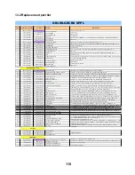
13.2 Replacement part list 
 

Item Maker Part Number

LGE P/N

Ref Des

Description

1

8M01-7119-B001

ACGK0136101

COVER ASSY,FRONT

Front cover Ass'y ( No.1~6 )

2

401-71190-0001

MCJK0106801

COVER,FRONT

Front cover

3

415-71190-0003

MFBB0031901

FILTER,RECEIVER

Receiver filter

4

415-71190-0002

MPBG0094101

PAD,LCD

LCM Sponge

5

415-71190-0001

MTAD0108701

TAPE,WINDOW

Main Lens tape, ADHESIVE_7119_TRANSPARENT_ADHESIVE_N/A_ADHESIVE FOR MAIN 

6

403-71190-0007

MWAC0120301

WINDOW,LCD

Main Lens

7

8M02-7119-S001

ACGM0135201

COVER ASSY,REAR

Rear cover +  Antenna protection tape + GSM Antenna ( No.7~14)

8

402-71190-0001

MCJN0104001

COVER,REAR

Rear Cabinet_7119_SILVER_PC_Painting_REAR CABINET_A-TEK PRECISION(SUZHOU)_N/A

9

415-71190-0007

MTAC0093601

TAPE,SHIELD

Antenna protection tape

10

330-0000-00147

SNGF0048701

ANTENNA,GSM,FIXED

GSM Antenna

11

405-71190-0003

MCCF0062201

CAP,MOBILE SWITCH

Cover_7119_BLACK_PORON_N/A_RF TEST PORT CAP_GUAN YI(WUJIANG)_N/A

12

405-71190-0001

MCCE0051101

CAP,RECEPTACLE

IO Cover

13

478-721000-014

MLAB0005401

LABEL,A/S

 WATER DISSOLVE LABEL_Mech. Label_7210_Global_WATER PROOF LABEL_N/A_E-

14

415-71190-0005

MPBZ0232401

PAD

PAD, Rear cover

15

320-0000-00047

SJMY0009301

VIBRATOR,MOTOR

Vibrator Bar Type_Y0408A-400350303-0021a_R2.25+4.40*4.60*13.40mm_LNLON_Spring contact type

16

327-0000-00073

SVLM0032001

LCD MODULE

1.5' , 65K color, LCD MODULE

17

409-00000-0068

GMZZ0027301

SCREW MACHINE

Screw ( 4ea for 1phone )

18

405-71200-0001

MCJA0089004

COVER,BATTERY

Battery cover

20

404-71190-0001

MKAG0016201

KEYPAD,MAIN

Standard Keypad. English

21

478-711500-001

MLAA0063202

LABEL,APPROVAL

IMEI label

22

8M08-7120-N001

SAFY0345101

PCB ASSY,MAIN

Main Board Ass'y_GB108 GRCBK (PCB ASSY, SMT + INSERT)

23

 415-71210-0006

MPBM0027001

RECEIVER FILTERMESH

FILTER_7121_BLACK_FELT MESH_N/A_RECEIVER FILTER_GUAN

24

415-71190-0006

MPBN0063401

SPEAKER CHAMBER SPONGE

GASKET_7119_BLACK_PORON_N/A_SPEAKER CHAMBER SPONGE_GUAN YI(WUJIANG)_ON 

25

313-0000-00129

SUSY0028301

Speaker & Receiver

RSPEAKER_YD-1813QT-1_13 * 18 mm_8   Ohm_93.0dB_CHANG ZHOU YU CHENG_± 

26

415-71190-0008

MTAZ0239701

LCM adhesive tape

ADHESIVE_7119_TRANSPARENT_ADHESIVE_N/A_LCM ADHESIVE_GUAN 

27

415-71210-0004

ADCA0090301

DOME ASSY,METAL

DOME_7121_NoColor_STAINLESS STEEL_N/A_METAL DOME_PRINTEC_N/A

28

312-0000-00040

SUMY0012301

Microphone

Omni-MIC._SOM4013S-Z422-C3310_58 'dB_- 42dB_± 2.0dB_

Φ

4.0*1.30mm_NA_SMD

29

415-71210-0003

MFBD0034601

Microphone Mesh

FILTER_7121_BLACK_FELT MESH_N/A_MIC MESH_GUAN YI(WUJIANG)_N/A

30

415-71210-0012

MIDZ0191901

LCM Connector Protection tape

SHEET_7121_BLACK_PET_N/A_MYLAR FOR LCM CONN_GUAN YI(WUJIANG)_N/A

31

309-0000-00021

EDLH0015001

LED

LED Single Color_LTST-C193TBKT-5A_BLUE_2pin_0603_5mA/18~28mcd_LITEON_Luminous Bin

32

309-0000-00111

EDSY0018501

Diode

Diode Schottky_SDM20U40-7_N/A_2pin_SOD-523_250mA/40V_DIODES_N/A

33

314-0000-00382

ENBY0048401

SIM card Connector

CON. SIM CARD CONNECTOR_SIM-06HB3G_2.540 mm_6 pin_OCTEKCONN_H=1.65mm

34

314-0000-00358

ENBY0048501

FPCB coneector

CON. FPC CONNECTOR_FH26W-13S-0.3SHW(05)_0.600 mm_13 pin_HIROSE_H=1.0mm

35

314-0000-00283

ENBY0048601

MMI 18pin Connector

CON. I/O FEMALE CONNECTOR_HSEJ-18S04-25R_0.400 mm_18 pin_HANSHIN_H=2.5mm

36

314-0000-00337

ENBY0048701

Battery Connector

CON. BATTERY CONNECTOR_BTP-03QE4G_3.000 mm_3 pin_OCTEKCONN_H=5.75 mm,Snap

37

314-0000-00070

ENBY0048801

RF CONNECTOR WITH SWITCH

CON. RF CONNECTOR WITH SWITCH_MM8430-2610RA1_3.000 mm_6 pin_MURATA_N/A

38

310-0000-00071

EQBP0011201

IC, NPN Transistor

NPN Epitaxial Planar Transistor_PDTC143ZE_3pin_SOT-416_PHILIPS_R1=4.7K, R2=47K

39

310-0000-00037

EQBP0011301

IC, MOSFET

N Channel-MOSFET_NTA4153NT1G_3pin_SC-75_ON SEMI_20V/915 mA

40

311-0000-00637

EUSY0376501

IC, BaseBand

I.C BASEBAND PROCESSOR_PMB7880_BGA_189 BALLS_NoMemory_INFINEON_N/A

41

311-0000-00638

EUSY0376601

IC, MCP

I.C FLASH MEMORY_S71GL032N40BFW0P0_FBGA_56 BA4M_SPANSION

42

311-0000-00689

EUSY0376701

IC, FM Module

I.C FM MODULE_SI4702-C19-GMR_QFN_20 PINS_NoMemory_SILICON LABS_N/A

43

311-0000-00689

EUSY0376801

IC, Audio Power Amp

I.C AUDIO POWER AMPLIFIER_TPA6202A1ZQVR_BGA_8 Balls_NoMemory_TI_Vo=3.6V, 0.63 W,

44

311-0000-00676

EUSY0377001

IC, Stereo audio power amp

I.C STEREO AUDIO POWER AMPLIFIER_TS486-IQT_DFN_8 PINS_NoMemory_ST_Po=3.3V,16

45

311-0000-00631

EUSY0377101

IC, Analog Switch, Dual SPDT

I.C ANALOG SWITCH_STG5223QTR_QFN_10 PINS_NoMemory_ST_DUAL SPDT

46

311-0000-00633

EUSY0377201

IC, DC-DC converter

I.C DC-DC CONVERT_MP9361DJ-LF-Z_TSOT-23_6 PINS_NoMemory_MPS_N/A

47

311-0000-00632

EUSY0377301

IC, Charge

I.C CHARGE_MP26021DQ-LF-Z_QFN_10 PINS_NoMemory_MPS_FOR Li-ion BATTERY,2.8V/1A

48

311-0000-00028

EUSY0377501

I.C POWER AMP MODULE(RF)

I.C POWER AMP MODULE(RF)_SKY77518-11_MCM_20
PINS NoMemory SKYWORKS 6*8*1 2mm

49

305-0000-00021

EXSY0023601

Crystal Ocsillator, 32.768KHz

Crystal Oscillator_Q-SPT7P0327620C5GL_32.768KHZ_±20ppm_SMD-7*1.5mm-4Pin_SII_CL=12.5pF

50

305-0000-00069

EXSY0023701

Crystal Ocsillator, 26MHz

Crystal Oscillator_EXS00A-CS00030_26.0 MHZ_±8.0ppm_SMD-3.2*2.5mm-4Pin_NDK_NX3225SA

51

415-71210-0007

MCBA0043901

SHIELD CAN, Cover and Frame

SHIELD CAN, Cover and Frame

52

326-0000-00117

SFSY0038501

Saw Filter

Filter SAW_B39182B9308G110_GSM 900 & 1800 2in1_EPCOS_FOR GSM RX,50/150 OHM-
SMD10PIN

53

479-00000-0048

MBAD0005204

BAG,VINYL(PE)

54

482-712000-001

MBEF0132913

BOX,UNIT

GB108 Standard Box

55

478-711500-001

 MLAC0003018

LABEL,BARCODE

56

475-7120GR-001

AMBA0153426

MANUAL ASSY,  warranty card

Manual Assy . Operation  Warranty card

57

306-0000-00079

SBPL0092203

BATTERY PACK,LI-ION

Li-ion Battery Cell Packing_3.7V_800mAh_BLACK_LGIP-431A-SBPL0092203_LG INNOTEK_Cell 

58

333-0000-00058

SGEY0003213

EAR PHONE/EAR MIKE SET

Headset Stereo Channel Type

59

331-0000-00098

SSAD0028201

ADAPTOR,AC-DC, EUROPE

Travel adapter, EUROPE

ADDITION

GB108.GRCBK SPPL

MAIN BOARD ASS'Y

Packing


Summary of Contents for GB108

Page 1: ...1 GB108 Service Manual LG Electronics ...

Page 2: ... 1 RF Trouble 41 4 2 TX Trouble 47 4 3 Power On Trouble 51 4 4 SIM Card Trouble 54 4 5 Vibrator Trouble 56 4 6 Keypad Trouble 58 4 7 RTC Trouble 60 4 8 Key Backlight Trouble 62 4 9 LCM Backlight Trouble 65 4 10 LCD Trouble 67 4 11 Microphone Trouble 69 4 12 Receiver Trouble 71 4 13 Speaker Trouble 73 4 14 Headphone Trouble 75 4 15 Charging Trouble 79 4 16 FM Radio Trouble 81 5 DOWNLOAD 86 5 1 Down...

Page 3: ... be responsible for any charges that result from such unauthorized use B Incidence of Harm If a telephone company determines that the equipment provided to customer is faulty and possibly causing harm or interruption in service to the telephone network it should disconnect telephone service until repair can be done A telephone company may temporarily disconnect service as long as repair is not don...

Page 4: ...ical equipment etc Interference from unsuppressed engines or electric motors may cause problems H Electrostatic Sensitive Devices ATTENTION Boards which contain Electrostatic Sensitive Devices ESD are indicated by the sign Following information is ESD handing Service personnel should ground themselves by using a wrist strap when exchange system boards When repairs are made to a system board they s...

Page 5: ...rd Shall support SIM card both 1 8V and 3V KEY Back Light Yes KEY Back Light color Blue 850 MHz class 4 2W 850 1900 N A 900 MHz class 4 2W 900 1800 1800 MHz class 1 1W 900 1800 Frequency 1900 MHz class 1 1W 850 1900 N A Standby Time Shall support minimum test minutes as min based on battery capacity of mAh 400 hrs 2 1mA 800mAh P P 5 Talk Time Shall support minimum test hours as hrs based on batter...

Page 6: ... Ring Vibrate Ring Vibrate Ring after vibrate Silent Y Earpiece Volume 6 Level Include Mute Y Audio Mute Y GSM dual band MS 900 1800 N Frequency Bands PCS dual band MS 850 1900 Configuration is during software compile time Y Circuit N Date Service Packet N Infrared IrDA N Bluetooth N USB N USB Mass storage N Connectivity RS232 UART Only for Phone tool download Y Voice Recording N Voice Command N V...

Page 7: ...e Y Auto Answer Y Auto Redial Y Calling Line Y Full Call Divert Y Speed Dialing Y Last Number Redial Y Multi Party Call Y Call Management ECT Explicit Call Transfer 4 Send Y Automatic Network Selection Y Manual Network Y Preferred Network Y Network Network Service Status Y DTMF Signaling Y DTMF DTMF Enable Disable Y Read Cell Broadcast Y On Off setting Receive On Off Y Alert setting Y Language set...

Page 8: ...al Calls except those directed to the Home PLMN Country Y BAIC Barring of All Incoming Calls Y BICRoam Barring of Incoming Calls when Roaming Outside the Home PLMN Country Y Supplementary Services Conference Call Up to 5 calls 1 Waiting Call Y Plug in Type 3V 1 8 V Y SIM Lock Service Provider Network Lock Hard Lock Y SIM SIM Toolkit Class 3 Y Read Message Y Write and Edit Message Y Send and Receiv...

Page 9: ...ry Charging Mode Y Language Selectable Auto Language Y Text Input Predictive word input T9 Y Calendar MAX 20 records 18 chars Y To Do N Scheduler Memo MAX 10 records 80 chars Y Setting Local Time Y Display Two Cities Time Dual Clock N Daylight saving World Time NITZ Y Unit converter Length Weight Volume Surface Velocity Temperature User defined Y Stop Watch Y Calculator Y Phone Book Sync Only For ...

Page 10: ...er Y Dimming Clock N Power off Alarm Y Real Time Clock On Alarm Event Y Mobile Tracking software For India Asia Y Others M DOG For China Y Micro SD Adapter N Accessory Stereo Ear mic without hook switch Ear mic type Stereo without hook key Only FM play supports Stereo Y ...

Page 11: ...11 3 TECHNICAL BRIEF Digital Main Processor Figure 3 1 PMB7880 FUNCTIONAL BLOCK DIAGRAM ...

Page 12: ...12 ...

Page 13: ...with fully integrated blocking filter Two integrated LNAs No need of interstage and IF filter Highly linear RF quadrature demodulator Programmable DC output level Very low power budget Transmitter Digital Sigma Delta modulator for GMSK modulation typical 163 5 dBc Hz 20 MHz Single ended outputs to PA Pout 3 5 dBm Very low power budget RF Synthesizer ΣΔSynthesizer for multi slot operation Fast lock...

Page 14: ... temperature battery voltage battery temperature and ambient temperature Differential microphone input System start up circuitry Charger circuitry for NiCd NiMh and LiIon cells Integrated regulators for direct connection to battery ...

Page 15: ...able gain amplifier The prefiltered and A to D converted voice signal forms a 2 Mbit s data stream The oversampled voice signal passes a digital decimation filter The E GOLDvoice performs speech and channel encoding including voice activity detection VAD and discontinuous transmission DTX and digital GMSK modulation In the RF transceiver part the baseband signal modulates the RF carrier at the des...

Page 16: ...1 14 Power Management The E GOLDvoice provides the power management unit PMU for the complete mobile phone application The integrated PMU is directly connected to the battery and provides a set of linear voltage regulators LDO s These LDO s generate all required supply voltages and currents needed in a low feature mobile phone A charger control circuit charges NiCd NiMH and LiIon batteries The cha...

Page 17: ...se the following mechanism Boot ROM flow Controls the boot transition to external flash Controls the flash update Flash tied to the individual chip via an ID using e fuses that is each E GOLDvoice chip has its own fused ID Further details on the E GOLDvoice security concept are not publicly documented 3 1 16 Asynchronous Operation Mode Concept The E GOLDvoice can operate in either The traditional ...

Page 18: ...T RF switches diplexer and a Power Amplifier Control PAC block with internal current sense resistor A custom BiCMOS integrated circuit provides the internal PAC function and decoder circuitry to control the RF switches The two Heterojunction Bipolar Transistor HBT PA blocks are fabricated onto a single Gallium Arsenide GaAs die One PA block supports the GSM900 band and the other PA block supports ...

Page 19: ...17 21 is a transmit and receive front end module FEM with Integrated Power Amplifier Control iPAC for dual band cellular handsets comprising GSM850 and PCS1900 operation Designed in a low profile compact form factor the SKY77517 21 offers a complete Transmit VCO to Antenna and Antenna to Receive SAW filter solution The FEM also supports Class 12 General Packet Radio Service GPRS multi slot operati...

Page 20: ...eceive modes are performed using two external control pads Refer to the functional block diagram in Figure 3 2 2 below The band select pad BS selects between GSM and PCS modes of operation The transmit enable TX_EN pad controls receive or transmit mode of the respective RF switch TX logic 1 Proper timing between transmit enable TX_EN and Analog Power Control VRAMP allows for high isolation between...

Page 21: ...XO This linearization unit computes the required digital control word out of the programmed AFC bits in order to have a linear pulling curve ppm vs AFC word The resulting digital control word DIG is filtered by a digital lowpass filter which can be scaled or deactivated using the bits DIGFILT0 and DIGFILT1 of the XO_INIT3 register The frequency correction splits into 2 parts 1 The XOCAL bits in th...

Page 22: ...22 RTC 32 768KHz Crystal Figure 3 4 E GoldVoice RTC Interface ...

Page 23: ...23 3 5 LCD Interface 3 wire SPI interface Figure 3 5 1 LCD Interface Figure 3 5 2 Charging PUMP Interface ...

Page 24: ...24 ...

Page 25: ...25 3 6 SIM Card Interface Figure 3 6 SIM CARD Interface ...

Page 26: ...26 3 7 KEYPAD Interface Figure 3 7 KEY MAXTRIX Interface ...

Page 27: ...27 3 8 Battery Charging Block Interface Figure 3 8 Charging IC Interface ...

Page 28: ...28 3 9 RF Interface Figure 3 9 RF Module SAW Filter Interface ...

Page 29: ...29 ...

Page 30: ...30 3 10 Audio Interface Figure 3 10 1 Audio Interface ...

Page 31: ...31 ...

Page 32: ...32 Figure 3 10 2 Main Speaker Receiver Interface ...

Page 33: ...33 Figure 3 10 3 Main Microphone Interface Figure 3 10 4 Headset Interface ...

Page 34: ...34 3 11 Key LED Interface Figure 3 11 Key LED Interface This handset has 8 LEDs that illuminates blue color Control signal is controlled by E GoldVoice with PWM and handset has 3 methods ON OFF Dimming ...

Page 35: ...35 3 12 Vibrator Interface Figure 3 12 Vibrator Interface This handset has Vibrator operation Control signal is controlled by E GoldVoice with PWM ...

Page 36: ...36 3 13 Memory Interface Figure 3 13 Memory Interface ...

Page 37: ...e Figure 3 1 E GOLDvoice Block Diagram That means all supply voltages needed are generated on chip with integrated linear voltage regulators The input of these linear voltage regulators is the battery voltage The externalmemory and SIM card supply is provided by the on chip voltage regulators Figure 3 14 2 is an overview of the internal generated supply voltages ...

Page 38: ...operation phases of the E GOLDvoice Current consumption during the standby mode is minimized by reducing the clock to 32 kHz and switching it off for most of the device In addition the power supply for the TEAKLite ROM is switched off and the controller RAM is switched to a power saving mode Start up and Reset Control State Machine Features Power up upon battery insertion push button alarm charger...

Page 39: ...39 3 15 FM Radio Interface GB105a b GB106 GB107a b GB108 only Figure 3 15 FM Radio Interface ...

Page 40: ...ally wraps around to the upper byte of register 00h and proceeds from there until continuous writes cease Data transfer ceases with the STOP command After every STOP command the internal address counter is reset For read operations the device acknowledge is followed by an eight bit data word shifted out on falling SCLK edges An internal address counter automatically increments to allow continuous ...

Page 41: ...41 ...

Page 42: ...42 PAM Matching component Mobile SW Antenna Matching component Antenna connect point ...

Page 43: ...43 ...

Page 44: ...44 ...

Page 45: ...45 ...

Page 46: ...46 ...

Page 47: ...47 ...

Page 48: ...48 TP2 TP1 TP3 ...

Page 49: ...49 TP2 TP1 TP3 ...

Page 50: ...50 ...

Page 51: ...uble Test Point Check Points Battery Voltage Need to over 3 35V Power On key detection PWRON signal Outputs of LDOs U101 EGV Voltage PART VBUF 2 8V TP1 VMEM 2 8V TP2 VIO 2 8V TP3 VSIM 2 85V TP4 VRF0 1 5V TP5 VANA 2 5V TP6 ...

Page 52: ...52 Circuit Diagram TP5 TP6 TP1 TP3 TP4 TP2 ...

Page 53: ...ge 3 35V Start Charge or Change Battery Push Power_ON key and check the level change of PWRON key Replace U101 Check the Voltage of LDOs Output U101 The Phone will Power LDO Voltage VBUF 2 8V VMEM 2 8V VIO 2 8V VSIM 2 85V VRF0 1 5V VANA 2 5V NO NO NO YES YES YES ...

Page 54: ...54 4 4 SIM Card Trouble Test Point Circuit Diagram ...

Page 55: ...y 2V or 3V SIM Card Does the SIM Card supports 2V or 3V Start Resolder J201 or other component Check solding status of J201 and other component R201 C203 C204 C205 Change Board Check TP1 2 85V NO NG NG YES YES Re download the SW Change Board Check Operation NO ...

Page 56: ...56 4 5 Vibrator Trouble Test Point Circuit Diagram ...

Page 57: ...57 Checking Flow Change Board Check Voltage Level of TP1 TP1 2 8V Start Change U506 Check Voltage level of TP2 0V NG NG OK OK Enter the Engineer Mode and set Vibrator ON Replace Vibrator ...

Page 58: ...58 4 6 Keypad Trouble Test Point Circuit Diagram ...

Page 59: ...59 Checking Flow Change Metal Dome Check Metal Dome Start Change PCB NG OK ...

Page 60: ...60 4 7 RTC Trouble Test Point Circuit Diagram ...

Page 61: ...ng Flow Replace X102 and try again Is the Frequency about 32kHz Start Replace C122 C123 Check soldering status of C122 C123 Replace C101 Check Voltage Level of TP1 2V RTC will work properly NO NO NO YES YES YES ...

Page 62: ...62 4 8 Key Backlight Trouble Test Point ...

Page 63: ...63 Circuit Diagram ...

Page 64: ...5 or Change PCB Check Voltage Level of TP1 2 8V Start Replace Component D501 D502 D503 D504 D505 R5 01 R507 R506 R508 R510 R513 Check LED Component D501 D502 D503 D504 D505 R 501 R507 R506 R508 R510 R51 3 NO NO YES YES Change PCB ...

Page 65: ...65 4 9 LCM Backlight Trouble Test Point Circuit Diagram ...

Page 66: ...66 Checking Flow Replace R408 or Change PCB Check Voltage Level of TP1 TP2 as 2 8V step waveform Start Replace U401 Check Voltage Level of TP3 as 4 9V step waveform NO NO YES YES Change PCB ...

Page 67: ...67 4 10 LCM Trouble Test Point Circuit Diagram ...

Page 68: ...g Flow Change PCB Backlight is OK Start Replace Component or LCM Check Control Signal and power including soldering status as the waveform NO NG YES OK Change PCB Replace J401 Check soldering status of J401 NG OK ...

Page 69: ...69 4 11 Microphone Trouble Test Point Circuit Diagram ...

Page 70: ...Start Replace U101 EGV Check Voltage Level of TP1 VMIC 2 5V Re solder or Replace Component Check Component status around Mic NO NG YES YES OK Replace U101 EGV or Change PCB Re solder or replace Microphone Check status of MIC NG OK ...

Page 71: ...71 4 12 Receiver Trouble Test Point Circuit Diagram ...

Page 72: ... the Component Check TP1 TP2 NG YES OK Replace U101 EGV or Change PCB Re solder or replace Receiver Check the Contact of Receiver NG OK Re solder or Replace Component Check Component status L301 L302 R303 R309 NG OK L301 L302 bias will fluctuate above 1 2V ...

Page 73: ...73 4 13 Speaker Trouble Test Point Circuit Diagram TP6 TP5 TP2 TP3 TP4 TP1 ...

Page 74: ...l of TP2 TP3 NO YES Try again or Change PCB Check the Battery Check the voltage level of TP1 VBAT NO YES Check U101 EGV Check the Level of TP4 High NO YES Re solder L301 L302 Check the signal of TP5 TP6 NO YES Re assemble or replace Speaker Check the Contact of Speaker NO ...

Page 75: ...75 4 14 Headphone Trouble Test Point ...

Page 76: ...76 Circuit Diagram TP1 TP2 ...

Page 77: ...e of the phone change to the earphone mode NO YES Re solder or replace the component Check voltage level of TP6 VMIC 2 5V Re solder causal component J501 Check component status around VMIC NO YES Earphone Check the signal level and HS_MIC Is it about 1 2 1 5VDC with a few tens mV AC Check U101 EGV NO YES YES MIC ...

Page 78: ...lace U101 EGV or Change the PCB Does waveform at TP3 U101 HS_REC fluctuate Re solder causal component J501 C322 etc Does waveform at TP4 TP5 U305 3 9 fluctuate YES Earphone YES Does waveform at TP1 TP2 J501 4 5 fluctuate NO Check U305 and component status around U305 ...

Page 79: ...79 4 15 Charging Trouble Test Point Circuit Diagram ...

Page 80: ...S Charging is properly operating NO Re solder the J501 pin12 13 VCHARGE I O Connector J501 is well soldered NO YES Replace the U503 The voltage of TP3 TP4 is over 2 5V NO YES Check the U101 EGV Check the voltage of TP5 is High or Low NO YES Battery is charged The battery may have problem Change the Battery YES ...

Page 81: ...81 4 16 FM Radio Trouble GB105a b GB106 GB107a b only Test Point ...

Page 82: ...82 Circuit Diagram ...

Page 83: ...oints TP1 2 3 Reasonable range 3 1V TP1 2 3 2 7V Give the additory solder in TP5 6 7 NO Replace the J501 Finish A condition is Good NO YES A condition is Good FM_Radio working is good NO YES Replace PCB A condition is Good INT FM or EXT FM ANT Check a condition of Ear Jack connector soldering J501 for Ext FM ANT INT FM B A ...

Page 84: ...s Good Check a condition of U303 soldering NO YES Replace U303 A condition is Good Check a condition of TP10 U304 Soldering NO YES Give the additory in TP10 U304 A condition is Good Check a condition of FM_Radio Performance Finish NO YES Replace PCB A condition is Good A ...

Page 85: ...er Matching component TP12 13 7 NO Give the additory solder in TP12 13 7 NO Replace the Z301 Finish A condition is Good YES A condition is Good FM_Radio working is good Check a condition of Pogo PIN for Z301 Int FM ANT TP11 INT FM B ...

Page 86: ...86 5 DOWNLOAD 5 1 Download Setup ...

Page 87: ...Stop download Ⓑ Selected configuration DLL file Ⓒ File name donwloading File F Exit X End program Setting S Configuration configuration download condition DLL SW files and etc About H MultiGSM Provide version information First select Setting Menu Ⓐ Ⓑ Ⓒ ...

Page 88: ...a appropriated DLL file You must select KP100_xxxxxx DLL file ⒷSelect files downloaded GB100 bin Ⓒ Select download speed You must 460800 System supports maximum 460800bps Ⓓ Select port select start and end port be operated Ⓐ Ⓑ Ⓒ Ⓓ ...

Page 89: ... download next step If configuration is finished then push start button and then button is changed to STOP Turn on power of multi download and connector phones If download is started then push start button else program will download repeatedly Ⓐ ...

Page 90: ...90 Download step 4 Ⓐ This region appears donwload status If download is finished PASS or FAIL message is showed Ⓐ ...

Page 91: ...91 6 BLOCK DIAGRAM ...

Page 92: ...92 ...

Page 93: ...93 ...

Page 94: ...94 ...

Page 95: ...95 ...

Page 96: ...96 ...

Page 97: ...97 ...

Page 98: ...98 8 BGA IC PIN Check BGA PIN Check of main chip Bottom view Use U101 Main chip PMB7880 Not Use EUSY0317401 ...

Page 99: ...99 BGA PIN Check of Memory Top View Use U201 Memory S71GL032N40BFW0P Not Use EUSY0328002 ...

Page 100: ...100 9 PCB LAYOUT ...

Page 101: ...Connector No Display U505 Key LED TR switch No LED J201 SIM connector No SIM VIB501 Vibrator PAD No Vibrator U506 Vibrator TR switch No Vibrator J502 Battery Connector No Charging No Power On U503Charging IC No Charging U304 FM Speaker AMP No sound Speaker or Headset U303 FM Tuner No FM radio X102 32 768KHz Crystal No Booting J501 I O Connector No Charging etc U301 Speaker AMP No Speaker ...

Page 102: ...Mode 1 Function Test 1 1 Test Purpose To verify handset functional is pass or fail when assembled by visual check 1 2 Test Facilities List 1 Battery 2 Earphone 3 Charger 4 GSM tester 4201S 5 Battery Cover 6 FM transmitter ...

Page 103: ...ED Illumination Vibrator Melody Vibrator function check Always on All keys function check Method 1 screen shows all icons for key and operator press key one by one then it disappear in screen Method 2 screen shows icon of key one by one then operator press it as phone instruction 3 Keyboard Receiver Receiver check 4 Audio Main Mic to Main Receiver audio loop check 5 Headsets Earpiece Aux Mic to Au...

Page 104: ...MMI 1 3 2 1 Service information Test Operator not need to insert test SIM card and enter to check Service information as below Service information Test Conducted Verifying item IMEI Check IMEI number Software version Read S W Number Version ...

Page 105: ...105 11 Calibration 11 1 Test equipment setup 11 2 Calibration Steps Execute HK_36 exe ...

Page 106: ...106 Click SETTING Menu Setup Logic operation such as the following figure PWR Power Supply CELL Call Test Equipment Setup UART Port Operation Mode 1 By Pass not control by GPIB 2 Normal control by GPIB ...

Page 107: ...107 Select MODEL Click START for RF calibration RF Calibration finish ...

Page 108: ...108 12 Stand alone test 12 1 Test program setting 12 1 1 Set COM port 12 1 2 Check PC Baud rate 115200 12 1 3 Confirm EEPROM Delta file prefix name ...

Page 109: ...109 12 1 4 Press power on key then click V24AT ON and then Update Info for communicating Phone and Test Program ...

Page 110: ...110 12 1 5 For the purpose of the Stand alone Test Change the phone to ptest mode and then click the Reset bar 12 1 6 Select Non signaling in the Quick Bar menu Then Stand alone Test set up finished ...

Page 111: ...ling mode bar and then confirm OK test in the command line 12 2 2 Put the number of TX channel in the ARFCN 12 2 3 Select TX in the RF mode menu and PCL in PA level menu 12 2 4 Finally Click Write All bar and try the efficiency test of phone ...

Page 112: ...112 12 3 RX Test 12 3 1 Put the number of RX channel in the ARFCN 12 2 2 Select RX in the RF mode menu 12 2 3 Finally Click Write All bar and try the efficiency test of phone ...

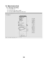
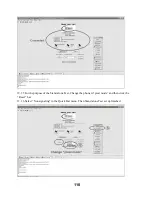
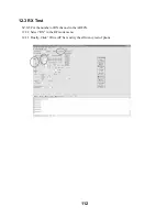
Page 113: ...113 13 EXPLODED VIEW REPLACEMENT PART LIST 13 1 Exploded View GB108 ...

Page 114: ...114 ...

Page 115: ...mA 40V_DIODES_N A 33 314 0000 00382 ENBY0048401 SIM card Connector CON SIM CARD CONNECTOR_SIM 06HB3G_2 540 mm_6 pin_OCTEKCONN_H 1 65mm 34 314 0000 00358 ENBY0048501 FPCB coneector CON FPC CONNECTOR_FH26W 13S 0 3SHW 05 _0 600 mm_13 pin_HIROSE_H 1 0mm 35 314 0000 00283 ENBY0048601 MMI 18pin Connector CON I O FEMALE CONNECTOR_HSEJ 18S04 25R_0 400 mm_18 pin_HANSHIN_H 2 5mm 36 314 0000 00337 ENBY004870...

Reviews: