


- 22 -
Copyright
2007LG Electronics. Inc. All right reserved.
Only for training and service purposes
LGE Internal Use Only
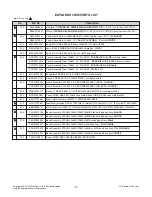
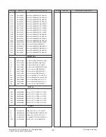
LOC. NO.
PART NO.
DESCRIPTION / SPECIFICATION
A1
SAB30967302
S/W Package[S-chassis L196/206/22
A2
6410TUW008A
"Power CordUL_CSA,LP-31 & SVT 18X3"
or 174-206M
Power CordSP305 IS14 SVT 18AWG 75
6410TPW003A
Power CordPG8B9CMCQ0A-062 LP-33 L
A3
3171TZ1099Q
S/W Package3171TZ1099Q Forte Mana
A4
68509F0003A
"Cable,AssemblyD-SUB TO D-SUB UL20"
A5
MBM37308501
CardPRINTING REGISTRATION BRAND L
C501
0CK104CF56A
"Capacitor,Ceramic,Chip0603B104K16"
C502
0CK473CH56A
"Capacitor,Ceramic,ChipC1608X7R1E4"
C503
0CK473CH56A
"Capacitor,Ceramic,ChipC1608X7R1E4"
C504
0CK473CH56A
"Capacitor,Ceramic,ChipC1608X7R1E4"
C505
0CK473CH56A
"Capacitor,Ceramic,ChipC1608X7R1E4"
C506
0CC102CK41A
"Capacitor,Ceramic,ChipC1608C0G1H1"
C507
0CK473CH56A
"Capacitor,Ceramic,ChipC1608X7R1E4"
C508
0CK473CH56A
"Capacitor,Ceramic,ChipC1608X7R1E4"
C509
0CC270CK41A
"Capacitor,Ceramic,ChipC1608C0G1H2"
C510
0CC270CK41A
"Capacitor,Ceramic,ChipC1608C0G1H2"
C511
0CK103CK51A
"Capacitor,Ceramic,Chip0603B103K50"
C512
0CK103CK51A
"Capacitor,Ceramic,Chip0603B103K50"
C513
0CK104CF56A
"Capacitor,Ceramic,Chip0603B104K16"
C514
0CK224CF56A
"Capacitor,Ceramic,Chip0603B224K16"
C515
0CE106CF638
"Capacitor,AL,RadialSHL5.0TP16VB10"
C516
0CK104CF56A
"Capacitor,Ceramic,Chip0603B104K16"
C517
0CK104CF56A
"Capacitor,Ceramic,Chip0603B104K16"
C518
0CK104CF56A
"Capacitor,Ceramic,Chip0603B104K16"
C519
0CK104CF56A
"Capacitor,Ceramic,Chip0603B104K16"
C520
0CK104CF56A
"Capacitor,Ceramic,Chip0603B104K16"
C521
0CK104CF56A
"Capacitor,Ceramic,Chip0603B104K16"
C522
0CK104CF56A
"Capacitor,Ceramic,Chip0603B104K16"
C523
0CK104CF56A
"Capacitor,Ceramic,Chip0603B104K16"
C524
0CK104CF56A
"Capacitor,Ceramic,Chip0603B104K16"
C525
0CK104CF56A
"Capacitor,Ceramic,Chip0603B104K16"
C526
0CK104CF56A
"Capacitor,Ceramic,Chip0603B104K16"
C527
0CK104CF56A
"Capacitor,Ceramic,Chip0603B104K16"
C528
0CK104CF56A
"Capacitor,Ceramic,Chip0603B104K16"
C529
0CK104CF56A
"Capacitor,Ceramic,Chip0603B104K16"
C530
0CK104CF56A
"Capacitor,Ceramic,Chip0603B104K16"
C531
0CK104CF56A
"Capacitor,Ceramic,Chip0603B104K16"
C532
0CK104CF56A
"Capacitor,Ceramic,Chip0603B104K16"
C533
0CK104CF56A
"Capacitor,Ceramic,Chip0603B104K16"
C534
0CK104CF56A
"Capacitor,Ceramic,Chip0603B104K16"
C535
0CK104CF56A
"Capacitor,Ceramic,Chip0603B104K16"
C536
0CK104CF56A
"Capacitor,Ceramic,Chip0603B104K16"
C537
0CK104CF56A
"Capacitor,Ceramic,Chip0603B104K16"
C538
0CK104CF56A
"Capacitor,Ceramic,Chip0603B104K16"
C539
0CC080CK11A
"Capacitor,Ceramic,ChipC1608C0G1H0"
C540
0CC080CK11A
"Capacitor,Ceramic,ChipC1608C0G1H0"
C541
0CC080CK11A
"Capacitor,Ceramic,ChipC1608C0G1H0"
C701
0CC101CK41A
"Capacitor,Ceramic,ChipC1608C0G1H1"
C702
0CC101CK41A
"Capacitor,Ceramic,ChipC1608C0G1H1"
C703
0CC680CK41A
"Capacitor,Ceramic,ChipC1608C0G1H6"
C704
0CK104CK56A
"Capacitor,Ceramic,Chip0603B104K50"
C705
0CC680CK41A
"Capacitor,Ceramic,ChipC1608C0G1H6"
C706
0CK104CF56A
"Capacitor,Ceramic,Chip0603B104K16"
C707
0CK104CF56A
"Capacitor,Ceramic,Chip0603B104K16"
C708
0CK104CF56A
"Capacitor,Ceramic,Chip0603B104K16"
C709
0CK104CF56A
"Capacitor,Ceramic,Chip0603B104K16"
C710
0CK104CF56A
"Capacitor,Ceramic,Chip0603B104K16"
C711
0CK104CF56A
"Capacitor,Ceramic,Chip0603B104K16"
C712
0CK104CF56A
"Capacitor,Ceramic,Chip0603B104K16"
C713
0CK104CF56A
"Capacitor,Ceramic,Chip0603B104K16"
C714
0CC680CK41A
"Capacitor,Ceramic,ChipC1608C0G1H6"
C715
0CC680CK41A
"Capacitor,Ceramic,ChipC1608C0G1H6"
C716
0CK104CF56A
"Capacitor,Ceramic,Chip0603B104K16"
C717
0CK104CF56A
"Capacitor,Ceramic,Chip0603B104K16"
C718
0CK104CF56A
"Capacitor,Ceramic,Chip0603B104K16"
C719
0CK104CF56A
"Capacitor,Ceramic,Chip0603B104K16"
C720
0CK104CF56A
"Capacitor,Ceramic,Chip0603B104K16"
C723
0CK104CF56A
"Capacitor,Ceramic,Chip0603B104K16"
C724
0CK105CD56A
"Capacitor,Ceramic,ChipC1608X7R1A1"
C725
0CC101CK41A
"Capacitor,Ceramic,ChipC1608C0G1H1"
C901
0CK103CK51A
"Capacitor,Ceramic,Chip0603B103K50"
C902
0CE107EF610
"Capacitor,AL,RadialKMG16VB100M 10"
C905
0CE107EF610
"Capacitor,AL,RadialKMG16VB100M 10"
C906
0CE107EF610
"Capacitor,AL,RadialKMG16VB100M 10"
C907
0CE107EF610
"Capacitor,AL,RadialKMG16VB100M 10"
C908
0CK104CK56A
"Capacitor,Ceramic,Chip0603B104K50"
C909
0CK104CK56A
"Capacitor,Ceramic,Chip0603B104K50"
C910
0CK104CK56A
"Capacitor,Ceramic,Chip0603B104K50"
C911
0CK102CK56A
"Capacitor,Ceramic,Chip0603B102K50"
C912
0CK102CK56A
"Capacitor,Ceramic,Chip0603B102K50"
C913
0CK102CK56A
"Capacitor,Ceramic,Chip0603B102K50"
C914
0CE227EF610
"Capacitor,AL,RadialKMG16VB220M 22"
C915
0CK103CK51A
"Capacitor,Ceramic,Chip0603B103K50"
C915
0CK105CD56A
"Capacitor,Ceramic,ChipC1608X7R1A1"
D701
0DS226009AA
"Diode,SwitchingKDS226 1.2V 85V 30"
D702
0DS226009AA
"Diode,SwitchingKDS226 1.2V 85V 30"
D703
0DS226009AA
"Diode,SwitchingKDS226 1.2V 85V 30"
D704
0DS226009AA
"Diode,SwitchingKDS226 1.2V 85V 30"
D705
0DS226009AA
"Diode,SwitchingKDS226 1.2V 85V 30"
D706
0DS226009AA
"Diode,SwitchingKDS226 1.2V 85V 30"
LOC. NO.
PART NO.
DESCRIPTION / SPECIFICATION
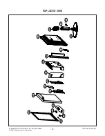
REPLACEMENT PARTS LIST
DATE: 2007. 06. 04.
CAPACITORs
DIODEs
ACCESSORY