


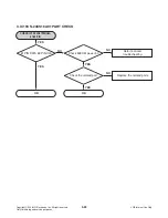


3-17
Copyright © 2008 LG Electronics. Inc. All right reserved.
Only for training and service purposes
LGE Internal Use Only
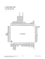
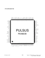
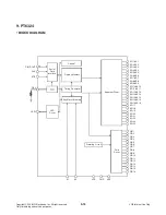
9. PT6324
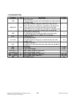
• PIN DESCRIPTION
Pin Name
I/O
Description
Pin No.
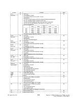
CLK I
Clock Input Pin
This pin reads serial data at the rising edge and outputs data at
the falling edge.
1
DIN/DOUT I/O
Data Input Pin/Data Output pin (N-Channel, Open-Drain)
When this pin acts as input pin, serial data is inputted at the
rising edge of the shift clock (starting from the lower bit)
When this pin acts as output pin, serial data is outputted at the
falling edge of the shift clock (starting from the lower bit)
2
STB I
Serial Interface Strobe Pin
The data input after the STB has fallen is processed as a
command. When this in is ìHIGHî, CLK is ignored.
3
LED1
O
LED Output Pin
4
K1 to K2
I
Key Data Input Pins
The data inputted to these pins is latched at the end of the
display cycle.
5, 6
OSC I
Oscillator Input Pin
A resistor is connected to this pin to determine the oscillation
frequency.
7
GND
-
Ground Pin
8, 52
VDD
-
Logic Power Supply
9, 51
SG1/KS1 to
SG16/KS16
O
High-Voltage Segment Output Pins
Also acts as the key source
10 to 25
SG17 to SG24
O
High-Voltage Segment Output Pins
26 to 33
GR1 to GR16
O
High-Voltage Grid Output Pins
34 to 49
VEE -
Pull-Down
Level
50