background image

- 12 -

LGE Internal Use Only

Copyright              LG Electronics. Inc. All right reserved. 
Only for training and service purposes

5. Manual Adjustment

5.1. ADC Adjustment

(1) Overview

ADC adjustment is needed to find the optimum black level
and gain in Analog-to-Digital device and to compensate
RGB deviation. 

(2) Equipment & Condition

1) Adjust Remocon
2) 801GF(802B, 802F, 802R) or MSPG925FA Pattern

Generator

- Resolution: 480i Comp1(MSPG-925FA: Model-209,

Pattern-65)

- Resolution: 1024*768 RGB(Inner Pattern)
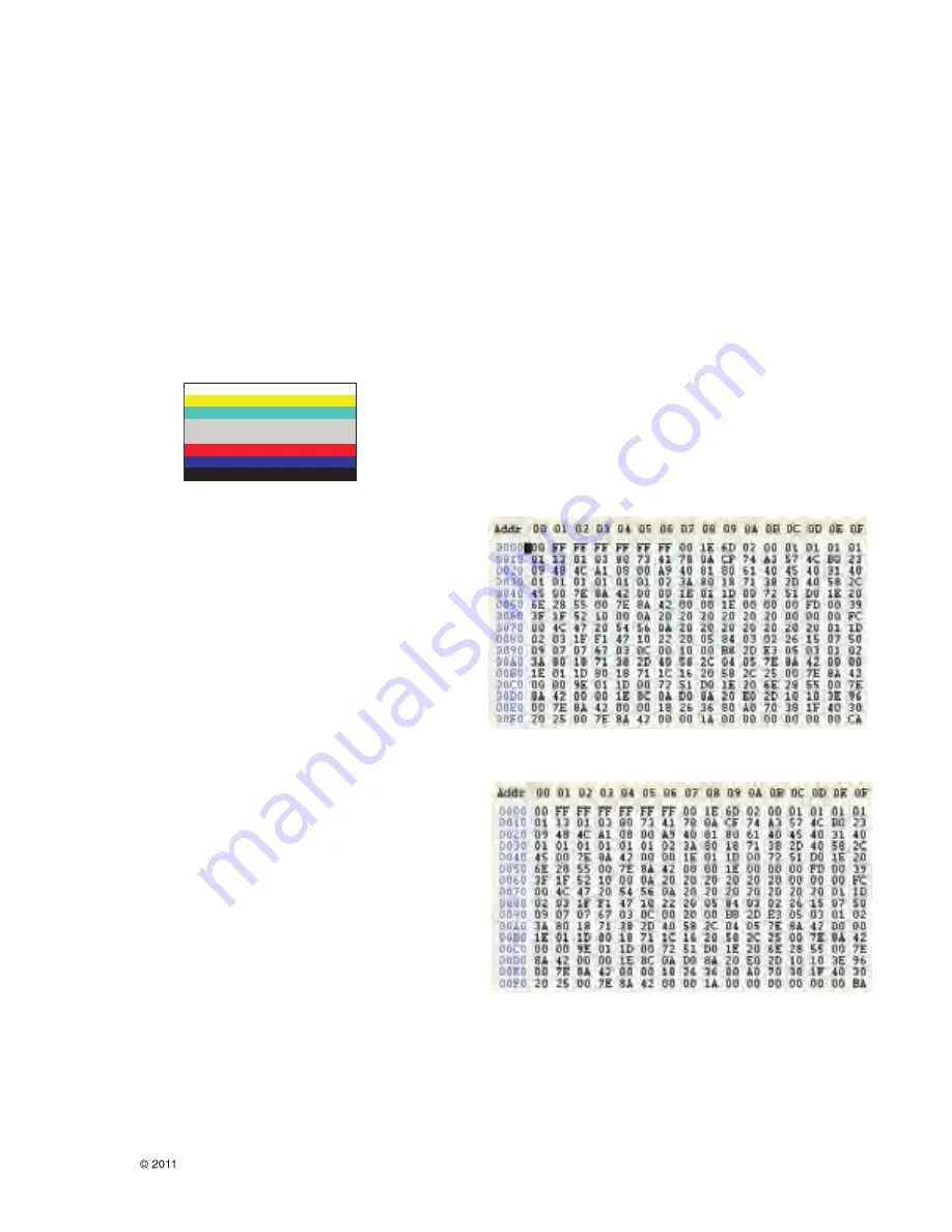
- Pattern : Horizontal 100% Color Bar Pattern
- Pattern level: 0.7±0.1 Vp-p
- Image

3) Must use standard cable

(3) Adjust method

•  ADC 480i/1080p Comp1, RGB 

1) Check connected condition of Comp1 cable to the

equipment 

2) Give a 480i Mode, Horizontal 100% Color Bar Pattern

to Comp1. 

(MSPG-925FA -> Model: 209, Pattern: 65) 

3) Change input mode as Component1 and picture mode

as “Standard” 

4) Press the In-start Key on the ADJ remote after at least

1 min of signal reception. Then, select 5.ADC 

Calibration. And Press OK Button on the menu “Start”.
The adjustment will start automatically. 

5) If ADC Comp 480i is successful, “ADC Component

Success” is displayed and Comp480i/1080p is
completed. 

If ADC calibration is failure, “ADC Component Fail” is
displayed. 

6) If ADC calibration is failure, after rechecking ADC

pattern or condition, retry calibration 

7) After completing  ADC Component, input mode will be

changed to RGB automatically. 

8) If ADC calibration is successful, “ADC RGB Success”

is displayed.  If ADC calibration is failure, “ADC RGB
Fail” is displayed. 

9) If ADC calibration is failure, after recheck ADC pattern

or condition, retry calibration 

5.2 EDID/DDC Download  

(1) Overview

It is a VESA regulation. A PC or a MNT will display an
optimal resolution through information sharing without any
necessity of user input. It is a realization of “Plug and Play”. 

(2) Equipment

• Adjust remocon. 
• Since embedded EDID data is used, EDID download JIG,

HDMI cable and D-sub cable are not need. 

(3) Download method

1) Press Adj. key on the Adj. R/C, 
2) Select EDID D/L menu. 
3) By pressing Enter key, EDID download will begin 
4) If Download is successful, OK is display, but If

Download is failure, NG is displayed. 

5) If Download is failure, Re-try downloads. 

•Caution) When EDID Download, must remove RGB/HDMI

Cable.

(4) EDID DATA 

1)LD450 Tool(FHD) 
• HDMI 1 EDID Table 

• HDMI 2 EDID Table 

Summary of Contents for EzSign 42LD452B

Page 1: ...EAD THE SAFETY PRECAUTIONS IN THIS MANUAL CHASSIS LA01Z MODEL 42LD452B 42LD452B UA North Latin America http aic lgservice com Europe Africa http eic lgservice com Asia Oceania http biz lgservice com Internal Use Only Printed in Korea P NO MFL66679907 1105 REV00 ...

Page 2: ...nal Use Only Copyright LG Electronics Inc All right reserved Only for training and service purposes 2 CONTENTS CONTENTS 2 SAFETY PRECAUTIONS 3 SPECIFICATION 6 ADJUSTMENT INSTRUCTION 11 EXPLODED VIEW 17 SVC SHEET ...

Page 3: ...perate without damage of electrical shock Leakage Current Cold Check Antenna Cold Check With the instrument AC plug removed from AC source connect an electrical jumper across the two AC plug prongs Place the AC switch in the on position connect one lead of ohm meter to the AC plug prongs tied together and touch other ohm meter lead in turn to each exposed metallic parts such as antenna terminals p...

Page 4: ...n your body by touching a known earth ground Alternatively obtain and wear a commercially available discharging wrist strap device which should be removed to prevent potential shock reasons prior to applying power to the unit under test 2 After removing an electrical assembly equipped with ES devices place the assembly on a conductive surface such as aluminum foil to prevent electrostatic charge b...

Page 5: ...e solder joints of the two original leads If they are not shiny reheat them and if necessary apply additional solder Fuse and Conventional Resistor Removal Replacement 1 Clip each fuse or resistor lead at top of the circuit board hollow stake 2 Securely crimp the leads of replacement component around notch at stake top 3 Solder the connections CAUTION Maintain original spacing between the replaced...

Page 6: ...20 minutes prior to the adjustment 3 Test method 1 Performance LGE TV test method followed 2 Demanded other specification Safety UL CSA IEC specification EMC FCC ICES IEC specification 6 SPECIFICATION NOTE Specifications and others are subject to change without notice for improvement 4 General Specification TV No Item Specification Remark 1 Receivable System 1 ATSC NTSC M 2 Available Channel VHF 0...

Page 7: ...lor Temperature Cool Typ 0 269 Typ The W B Tolerance is 0 015 0 273 0 015 0 015 for Adjustment Medium Typ 0 285 Typ 0 015 0 293 0 015 Warm Typ 0 313 Typ 0 015 0 329 0 015 No Item Min Typ Max Unit Remarks 1 Max Luminance 400 500 cd m2 Center 1 point Full White Pattern 2 Luminance uniformity 1 3 5point 3 Color coordinate RED X Typ 0 639 Typ Default Y 0 03 0 334 0 03 GREEN X 0 290 Y 0 606 BLUE X 0 14...

Page 8: ...attern 2 Luminance uniformity 1 3 5point 3 Color coordinate RED X Typ 0 640 Typ Default Y 0 03 0 330 0 03 GREEN X 0 281 Y 0 590 BLUE X 0 144 Y 0 060 WHITE X 0 280 Y 0 290 4 Contrast ratio 3200 4000 6 Color Temperature Cool Typ 0 269 Typ The W B Tolerance is 0 015 0 273 0 015 0 015 for Adjustment Medium Typ 0 285 Typ 0 015 0 293 0 015 Warm Typ 0 313 Typ 0 015 0 329 0 015 5 3 42LD450C UA T420HW06 V0...

Page 9: ...1080 67 500 60 148 50 HDTV 10 1920 1080 67 432 59 94 148 352 HDTV 11 1920 1080 27 000 24 000 74 25 HDTV 12 1920 1080 26 97 23 976 74 176 HDTV 13 1920 1080 33 75 30 000 74 25 HDTV 14 1920 1080 33 71 29 97 74 176 HDTV 7 RGB Input PC No Resolution H freq kHz V freq kHz Pixel clock Proposed PC DDC 1 640 350 31 468 70 09 25 17 EGA X 2 720 400 31 469 70 08 28 32 DOS O 3 640 480 31 469 59 94 25 17 VESA V...

Page 10: ...2 60 015 85 50 VESA WXGA X 8 1280 1024 63 981 60 020 108 00 VESA SXGA O 9 1600 1200 75 00 60 00 162 VESA UXGA O 10 1920 1080 67 5 60 148 5 HDTV 1080P O DTV 1 720 480 31 5 60 27 027 SDTV 480P 2 720 480 31 47 59 94 27 00 SDTV 480P 3 1280 720 45 00 60 00 74 25 HDTV 720P 4 1280 720 44 96 59 94 74 176 HDTV 720P 5 1920 1080 33 75 60 00 74 25 HDTV 1080I 6 1920 1080 33 72 59 94 74 176 HDTV 1080I 7 1920 10...

Page 11: ... items can be check using In Star Menu 1 ADJUST CHECK Component 1080p and RGB PC Adjust will be calculated by 480i adjust value 3 2 Final assembly adjustment White Balance adjustment RS 232C functionality check Factory Option setting per destination Ship out mode setting In Stop 3 3 Etc Ship out mode Service Option Default USB Download S W Update Option Service only ISP Download Optional 4 Automat...

Page 12: ...ADC Comp 480i is successful ADC Component Success is displayed and Comp480i 1080p is completed If ADC calibration is failure ADC Component Fail is displayed 6 If ADC calibration is failure after rechecking ADC pattern or condition retry calibration 7 After completing ADC Component input mode will be changed to RGB automatically 8 If ADC calibration is successful ADC RGB Success is displayed If ADC...

Page 13: ...t 1 Color Analyzer CA 210 NCG CH 9 WCG CH12 2 Adj Computer During auto adj RS 232C protocol is needed 3 Adjust Remocon 4 Video Signal Generator MSPG 925F 720p 216 Gray Model 217 Pattern 78 Only when internal pattern is not available Color Analyzer Matrix should be calibrated using CS 1000 3 Equipment connection MAP 4 Adj Command Protocol 1 RS 232C Command used during auto adj Ex wb 00 00 Begin whi...

Page 14: ...Z Adj menu 6 White Balance you can select one of 2 Test pattern ON OFF Default is inner ON By selecting OFF you can adjust using RF signal in 216 Gray pattern Adj condition and cautionary items 1 Lighting condition in surrounding area Surrounding lighting should be lower 10 lux Try to isolate adj area into dark surrounding 2 Probe location LCD Color Analyzer CA 210 probe should be within 10cm and ...

Page 15: ...s fully inserted to the SET If loose re insert 2 Perform GND Internal Pressure auto check Unit fully inserted Power cord Antenna cable and A V arrive to the auto check process Connect D terminal to AV JACK TESTER Auto CONTROLLER GWS103 4 ON Perform GND TEST If NG Buzzer will sound to inform the operator If OK changeover to I P check automatically Remove CORD A V form AV JACK BOX Perform I P test I...

Page 16: ... files from memory 4 Updating is staring 5 Updating Completed The TV will restart automatically 6 If your TV is turned on check your updated version and Tool option explain the Tool option next stage If downloading version is more high than your TV have TV can lost all channel data In this case you have to channel recover if all channel data is cleared you didn t have a DTV ATV test on production ...

Page 17: ... and mechanical parts in this chassis have special safety related characteristics These parts are identified by in the Schematic Diagram and EXPLODED VIEW It is essential that these special safety parts should be replaced with the same components as recommended in this manual to prevent X RADIATION Shock Fire or other Hazards Do not modify the original design without permission of manufacturer IMP...

Page 18: ...47_FHD R636 5 1 180K 1 TCON_47_FHD R635 5 220K TCON_47_FHD 1 R611 5 27K 1 TCON_55_FHD R637 6 150K TCON_55_FHD 1 R643 6 180K TCON_55_FHD 1 R609 6 68K 1 TCON_55_FHD R610 6 56K TCON_55_FHD 1 R611 6 510K 1 TCON_55_FHD R620 6 27K 1 TCON_55_FHD R622 6 68K 1 TCON_55_FHD R621 6 150K 1 TCON_55_FHD R635 6 75K TCON_55_FHD 1 R636 6 15K 1 TCON_55_FHD R641 6 27K 1 TCON_42_FHD R637 3 150K TCON_42_FHD R643 3 1 TH...

Page 19: ...ASZ A11 A_DDR3_BA2 DDR2_A5 A23 A_DDR3_MCLK DDR2_MCLK A12 A_DDR3_MCLKZ DDR2_MCLKZ C11 A_DDR3_CKE DDR2_DQ5 B12 A_DDR3_ODT DDR2_ODT C20 A_DDR3_RASZ DDR2_WEZ A20 A_DDR3_CASZ DDR2_BA1 B20 A_DDR3_WEZ DDR2_BA0 A21 A_DDR3_RESETB C22 A_DDR3_DQSL DDR2_DQS0 C16 A_DDR3_DQSLB DDR2_DQSB0 B16 A_DDR3_DQSU DDR2_DQSB1 A16 A_DDR3_DQSUB DDR2_DQS1 C15 A_DDR3_DML DDR2_DQ13 A14 A_DDR3_DMU DDR2_DQ6 B18 A_DDR3_DQL0 DDR2_D...

Page 20: ...SDB_DEMOD 1 2V_DE 0 1uF C2902 ISDB_DEMOD 0 1uF C2908 ISDB_DEMOD 22 R2913 ISDB_DEMOD FE_TS_SYNC TP2906 ISDB_DEMOD 0 1uF C2903 ISDB_DEMOD 25MHz X2901 ISDB_DEMOD 10K 1 R2903 ISDB_DEMOD 0 1uF 16V C2923 ISDB_DEMOD 0 1uF C2910 ISDB_DEMOD FE_TS_VAL_ERR 2 2K R2914 OPT TP2904 ISDB_DEMOD TP2907 ISDB_DEMOD DEMOD_SCL 0 1uF 16V C2924 ISDB_DEMOD 0 1uF 16V C2917 ISDB_DEMOD 2 2K R2905 ISDB_DEMOD DEMOD_RESET 10K R...

Page 21: ...GND 11 VIDEO 2 BST_CNTL 10 NC 4 NC RF_AGC 1 ANT_PWR OPT 17 DIF_1 9 SIF 8 NC IF_TP 3 B 16 IF_AGC_CNTL 7 SDA 6 SCL 15 RESET 18 DIF_2 SHIELD 19 IF_P_MSTAR 1K R5022 3 3V_Normal 22uF 16V C5019 IF_N_MSTAR 0 BOOSTER_OPT R5014 LNA2_CTL 470 R5029 RF_SWITCH_CTL 3 3V_TU 0 1uF 16V C5031 22uF 16V C5020 0 TU_CVBS_BYPASS R5039 IF_N_EXT 82 R5032 TU_SDA IF_AGC 10K BOOSTER_OPT R5019 0 1uF 16V C5025 100K R5011 0 1uF...

Page 22: ...2 33 34 35 36 37 38 39 40 41 42 GMA7 RXA2 POL RXDCK RXC4 0 NON_GIP R768 RXBCK RXBCK GMA6 CLK4 VCOMRFB 0 R716 WAFER_HD VGL 5V RXA1 0 GIP R729 GMA13 PANEL_VCC 0 NON_GIP R772 33 R708 240Hz 3D 3 3K R700 MINI_LVDS 0MINI_LVDS R754 PANEL_VCC GMA16 PANEL_VCC RXA3 33 R706 240Hz 0 01uF 50V C708 MINI_LVDS PWM_DIM GMA12 RXA4 RXA2 VCC_LCM RXB2 GMA4 RXC4 RXA0 GMA4 RXA1 PWM_DIM OPC_EN RXB4 RXA3 VCC_LCM GMA9 VDD_...

Page 23: ... 22 MONITOR0 23 MONITOR1 24 MONITOR2 25 FAULT 26 VDR2B 27 BST2B 28 PGND2B_1 29 PGND2B_2 30 OUT2B_1 31 OUT2B_2 32 PVDD2B_1 33 PVDD2B_2 34 PVDD2A_1 35 PVDD2A_2 36 OUT2A_1 37 OUT2A_2 38 PGND2A_1 39 PGND2A_2 40 BST2A 41 VDR2A 42 NC 43 VDR1B 44 BST1B 45 PGND1B_1 46 PGND1B_2 47 OUT1B_1 48 OUT1B_2 49 PVDD1B_1 50 PVDD1B_2 51 PVDD1A_1 52 PVDD1A_2 53 OUT1A_1 54 OUT1A_2 55 PGND1A_1 56 PGND1A_2 57 EP_PAD 4 7K...

Page 24: ...RING 4 R_SPRING 7A B_TERMINAL1 6A T_TERMINAL1 3 E_SPRING 0 R1021 0 R1017 3 5V_ST 510 R166 2 2uF 16V C120 510 R164 3 9K R163 47uF 25V C114 10K R114 5 1V D104 10K R130 0 0 1 u F C117 AO3407A Q102 G D S RJP_CTRL3 008 AR28 MJ 657PT 8 SD JK1105 1 1 2 2 3 3 4 4 5 5 6 6 7 7 8 8 9 9 RJP_CTRL4 008 AE21 510 R153 OPT 12V 15V 3 9K R152 0 0 1 u F C116 0 0 1 u F C119 5 1V D101 5 1V D103 5 1V D102 510 R154 3 3V_...

Page 25: ..._SIDE 14 13 5 D1_GND 20 JACK_GND 12 11 2 D2_GND 19 18 10 CK 4 D1 1 D2 17 9 D0 8 D0_GND 3 D2 16 7 D0 6 D1 15 BSS83 Q805 S B D G 68K R892 3 5V_ST 68K R853 CEC_ON OFF GND 68K R854 68K OPT R857 0 OPT R855 0 1uF 16V C805 AVRL161A1R1NT OPT D803 D804 10K R856 GND BSS83 Q806 S B D G 3 3V_Normal 0 R858 CEC_REMOTE_S7 SCART1_Rout TP3805 TP3806 DTV MNT_VOUT TP3802 SC1_FB SCART1_MUTE TP3801 TP3804 TP3803 TP380...

Page 26: ...P C677 VGH 25V VGH_M 25V 47K R605 OPT VGH 25V 10 R633 GIP 10 R630 GIP OPT R603 OPT 0 GIP R696 1M NON_GIP R698 10uF 16V C661 REF REF 10K R632 GIP 0 R627 1uF C617 50V 10 R629 GIP 10 R631 GIP EN2 1K R613 EN2 EN2 MMSD4148T1G 100V D606 OPT MMSD4148T1G 100V D607 VDD_LCM 16V 0 R638 OPT 200 NON_GIP R631 1 200 NON_GIP R629 1 12505WS 03A00 P700 URSA_DEBUG 1 2 3 4 AMP_SCL AMP_SDA 1uF 10V C651 1uF 50V C606 10...

Page 27: ... 10K 1 R2405 12507WR 12L P2401 1 2 3 4 5 6 7 8 9 10 11 12 13 47K R2425 2SC3052 Q2406 E B C 47K R2429 10K R2430 47K R2431 22 R2428 3 5V_ST 2SC3052 Q2405 E B C 3 5V_ST IR 3 5V_ST 3 3K OPT R2426 0 OPT R2427 NEC_EEPROM_SCL NEC_EEPROM_SDA 1 5K R2414 1 5K R2413 JP2407 JP2408 JP2409 JP2410 JP2411 5 6B D2403 5 6B D2404 5 6B D2405 0 R1153 3 5V_ST 0 R1154 NEC_RXD Q1002 E B C 0 1uF C1105 100 R1124 3 5V_ST 30...

Page 28: ...09 3 5V_ST MODEL1_OPT_3 22 R1037 2SC3052 Q1001 E B C NEC_ISP_Rx GND 22 R1069 3 5V_ST MODEL1_OPT_1 MICOM_RESET 0 1 u F C1002 OLP RF_RESET 4 7K R1014 47K R1001 TP1002 22 R1054 19 22_LAMP LED_B LG_LOGO 22 R1039 100 R1070 FLMD0 NEC_EEPROM_SDA NEC_SDA INV_CTL NEC_EEPROM_SDA TP1003 10K R1005 AMP_MUTE NEC_ISP_Rx AMP_RESET_N NEC_ISP_Tx MICOM_RESET 22 R1049 OPT PANEL_CTL KEY2 OCD1A 10K R1072 22 R1063 MODEL...

Page 29: ...425 NR8040T3R6N 3 6uH L415 RT1P141C T112 Q402 1 2 3 MP8706EN C247 LF Z IC401 3 SW_2 2 SW_1 4 BST 1 IN 5 EN SYNC 6 FB 7 VCC 8 GND 1uF 25V OPT C419 10K R445 NCP803SN293 IC408 ON SEMI 1 GND 3 VCC 2 RESET 10K R459 100 R480 PD_ 12V 4 7uF 16V C443 FW20020 24S P403 NORMAL_EXPEPT_32 19 14 9 4 18 13 8 3 17 12 7 2 16 11 6 1 20 15 10 5 21 22 23 24 0 POWER_18_A_DIM R451 0 POWER_20_A_DIM R453 1uF 25V OPT C484 ...

Page 30: ..._7 M1 VSS_8 M9 VSS_9 P1 VSS_10 P9 VSS_11 T1 VSS_12 T9 VSSQ_1 B1 VSSQ_2 B9 VSSQ_3 D1 VSSQ_4 D8 VSSQ_5 E2 VSSQ_6 E8 VSSQ_7 F9 VSSQ_8 G1 VSSQ_9 G9 0 R327 0 R328 H5TQ1G63BFR H9C IC301 1 FRC_DDR_1333 A0 N3 A1 P7 A2 P3 A3 N2 A4 P8 A5 P2 A6 R8 A7 R2 A8 T8 A9 R3 A10 AP L7 A11 R7 A12 BC N7 A13 T3 A15 M7 BA0 M2 BA1 N8 BA2 M3 CK J7 CK K7 CKE K9 CS L2 ODT K1 RAS J3 CAS K3 WE L3 RESET T2 DQSL F3 DQSL G3 DQSU C...

Page 31: ...F2 A_RX0P G2 A_RX0N G3 A_RX1P H3 A_RX1N G1 A_RX2P H1 A_RX2N H2 DDCDA_DA GPIO24 F5 DDCDA_CK GPIO23 F4 HOTPLUGA GPIO19 E6 B_RXCP D3 B_RXCN C1 B_RX0P D1 B_RX0N D2 B_RX1P E2 B_RX1N E3 B_RX2P F3 B_RX2N E1 DDCDB_DA GPIO26 D4 DDCDB_CK GPIO25 E4 HOTPLUGB GPIO20 D5 C_RXCP AA2 C_RXCN AA1 C_RX0P AB1 C_RX0N AA3 C_RX1P AB3 C_RX1N AB2 C_RX2P AC2 C_RX2N AC1 DDCDC_DA GPIO28 AB4 DDCDC_CK GPIO27 AA4 HOTPLUGC GPIO21...

Page 32: ...P LVSYNC AE26 RLV0N LHSYNC AE25 RLV1N LCK AF26 RLV2P RED 9 AF25 RLV1P LDE AE24 RLV2N RED 8 AF24 RLV4P RED 5 AF23 RLV4N RED 4 AD22 RLV5P RED 3 AE22 RLV5N RED 2 AF22 TCON3 OE GOE GCLK2 AD19 TCON15 SCAN_BLK1 AE19 TCON18 CS7 GCLK5 AD21 TCON19 CS8 GCLK6 AE21 TCON11 CS5 HCON AF21 TCON10 CS4 OPT_N AD20 TCON9 CS3 OPT_P AE20 TCON16 WPWM AF20 TCON12 DPM AF19 TCON1 STV GSP VST AD18 TCON5 TP SOE AE18 TCON14 S...

Page 33: ..._DATA 0 7 FE_TS_CLK PCM_A 7 PCM_WAIT CI_TS_DATA 0 PCM_A 3 PCM_A 11 PCM_A 13 CI_TS_DATA 2 PCM_A 4 PCM_A 14 CI_TS_CLK CI_TS_DATA 1 PCM_A 6 PCM_A 0 PCM_IORD EPHY_REFCLK TP2103 TP2109 TP2106 TP2111 TP2108 EPHY_TXD0 ET_RXER EPHY_MDIO TP2107 TP2102 EPHY_CRS_DV TP2105 EPHY_RXD0 EPHY_MDC TP2110 EPHY_RXD1 TP2104 RST_PHY TP2101 EPHY_TXD1 EPHY_EN TP2501 RF_ENABLE M_REMOTE_TX TP2503 TP2504 M_REMOTE_RX TP2502 ...

Page 34: ......

Page 35: ...gnal Block Audio Signal Block Flash Block Reset Flash Block Reset I2C Block I2C Block GPIO Block GPIO Block POWER Block POWER Block Overall Block Diagram Overall Block Diagram LVDS 출력 Block LVDS 출력 Block Copyright ⓒ 2010 LG Electronics Inc All right reserved Only for training and service purposes LGE Internal Use Only ...

Page 36: ...b Pr L R CVBS L R CS RE WE Audio L R Audio L R for RGB HDMI 2 side HDMI SPDIF DP DM 5V RX TX RX TX Micom UPD78F0513AGA 24MHz JACK PACK JACK PACK at REAR at REAR SCL SDA_3 3V LVDS RF S7 LGE101D S7 T LGE105 RS 232C CTRL SVC S W Reset TDVJ H001F Audio L R H P LCD Module FHD 60Hz LCD Module FHD M S 60Hz Mini LVDS P Gamma Power Shift Power Control I2C SCL SDA RJP GPIO IR_IN IR_IN L R OUT External Speak...

Page 37: ...OMP1_Y COMP1_Pr COMP1_Pb AV_CVBS_IN SIDEAV_CVBS_IN RXCAKP RXCAKN RXA0P RXA0N RXA1P RXC1N RXA2P RXA2N D2 _HDMI1 D1 _HDMI1 D0 _HDMI1 CK _HDMI1 CEC_REMOTE CEC_REMOTE D2 _HDMI4 D1 _HDMI4 D0 _HDMI4 CK _HDMI4 IF_AGC RXCCKP RXCCKN RXC0P RXC0N RXC1P RXC1N RXC2P RXC2N RF TDVJ H001F TU_SIF TU_CVBS IF Copyright ⓒ 2010 LG Electronics Inc All right reserved Only for training and service purposes LGE Internal U...

Page 38: ...IDEAV_L_IN PC_R_IN PC_L_IN Digital AMP NTP7000N SPDIF_OUT 3 3V 1K Audio L Audio R HP_ROUT HP_LOUT IP IF IFAGC SIFP CVBS0P IF_AGC RF TU_SIF TU_CVBS IF TDVJ H001F I2S_OUT_MCK I2S_SCK I2S_LCRK I2S_MASTER_CLK I2S_LCRH I2S_OUT_BCK I2S_OUT_WS I2S_OUT_SD Copyright ⓒ 2010 LG Electronics Inc All right reserved Only for training and service purposes LGE Internal Use Only ...

Page 39: ... PF_OE PF_CE0 PF_CE1 PF_ALE PF_WE RB RE CE CLE ALE WE I O 0 I O 1 I O 2 I O 3 I O 4 I O 5 I O 6 I O 7 8 PCM_A 0 7 WP PF_AD15 F_RB PF_OE PF_CE0 PF_CE1 PF_ALE PF_WE PF WP Reset Switch Micom UPD78F0513AGA SOC_RESET HWRESET 3 3V 3 5V_ST Copyright ⓒ 2010 LG Electronics Inc All right reserved Only for training and service purposes LGE Internal Use Only ...

Page 40: ... IC501 AMP_SCL SDA EEPROM CAT24WC08W IC103 22 ohm 22 ohm Micom UPD78F0513AGA IC1002 EEPROM AT24C512BW IC1001 GPIO 174 GPIO 175 NEC_SCL SDA 22 ohm 22 ohm 3 3V_Nor 3 2k ohm 3 3k ohm 3 3V_Nor 3 2k ohm 3 3k ohm TGPIO0 TGPIO1 MAX9668ETP P GAMMA IC1601 33ohm 33 ohm TGPIO2 TGPIO3 Tuner TDVJ H001F TU5001 33ohm 33 ohm 22 ohm 22 ohm EEPROM AT24C02BN8 IC801 IC804 DDCDA_CK DDCDC_CK 22 ohm 22 ohm RGB_DDC_SCL S...

Page 41: ...1 TCON8 RS232C MAX3232CDR UART_RX2 S7_RXD UART_TX2 S7_TXD 5V_HDMI_4 P403 or P402 POWER WAFER PWM2 PWM_DIM A_DIM PWM0 USB_DM1 USB_DM USB_DP1 USB_DP JK1204 USB JACK Error_DET GPIO 41 GPIO 8 PM2 GPIO143 TCON0 GPIO147 TCON4 R2619 R2618 Copyright ⓒ 2010 LG Electronics Inc All right reserved Only for training and service purposes LGE Internal Use Only ...

Page 42: ... USB1_OCD 50 PWM3 GPIO69 G22 SC_RE2 51 PWM4 GPIO70 G21 SC_RE1 103 GPIO51 UART1_TX F19 M_REMOTE_TX 104 GPIO50 UART1_RX F20 M_REMOTE_RX 52 SAR0 GPIO31 C6 DSUB_DET 53 SAR1 GPIO32 B6 MODEL_OPT_ 105 GPIO42 G19 MODEL_OPT_0 54 SAR2 GPIO33 C8 PCM_5V_CTL 106 GPIO41 G20 ERROR_OUT 55 SAR3 GPIO34 C7 RST_PHY 107 GPIO40 M20 SC1 COMP1_DET 56 SAR4 GPIO35 A6 RST_HUB 108 GPIO39 L20 FRC_RESET 109 GPIO38 K20 ET_RXER ...

Page 43: ... AMP NTP3100L RS232C MAX3232CDR RXD0 NEC_RXD TXD0 NEC_TXD AMP_MUTE P403 or P402 POWER WAFER INT_CTL RL_ON R2619 R2618 P74 P73 P71 P140 KEY1 KEY2 ANI6 ANI7 IR INTP5 Copyright ⓒ 2010 LG Electronics Inc All right reserved Only for training and service purposes LGE Internal Use Only ...

Page 44: ...18 P14 RXD6 NEC_ISP_Rx 19 P13 TXD6 NEC_ISP_Tx 20 P12 SO10 POWER_ON OFF2_2 21 P11 SL10 RXD0 NEC_RXD 22 P10 SCK10 TXD0 NEC_TXD 25 ANI7 P27 KEY1 26 ANI6 P26 KEY2 27 ANI5 P25 SIDE_HP_MUTE 28 ANI4 P24 OLP 29 ANI3 P23 POWER_ON OFF1 30 ANI2 P22 MODEL1_OPT_2 31 ANI1 P21 MODEL1_OPT_3 32 P20 ANI0 SCART1_MUTE 33 P130 WIRELESS_SW_CTRL 34 P01 TI010 TO00 EDID_WP 35 P00 TI000 OPC_EN 36 P140 PCL INTP6 RL_ON 37 P1...

Page 45: ...출력 Block 32 37 P801 30pin LVDS Wafer HD 60Hz LGD 19 22 LVDS TXA0 LVDS TXA1 LVDS TXA2 LVDS TXAC LVDS TXA3 Panel_Vcc 12V LVDS OUT Block Copyright ⓒ 2010 LG Electronics Inc All right reserved Only for training and service purposes LGE Internal Use Only ...

Page 46: ...2 LVDS RXB3 LVDS RXB4 LVDS RXA0 LVDS RXA1 MAX17113 4CH DCDC converter IC603 TPS62110 DCDC converter IC600 MAX9668 P_GAMMA Vcom IC601 MAX17119 Level shifter IC602 Vgh_28V Vdd_16V Vcc_3 3V Vgl_ 5V Panel_Vcc 12V Enable1 For VGL Enable2 For VGH VDD Panel_Vcc 12V Enable2 For HVDD HVDD VDD_EVEN ODD VST GCLK2 4 VDD_EVEN_ODD VST 33V level AMP_SDA AMP_SCL GCLK VDD_EVEN_ODD VST 33V level T_con signal POL SO...

Page 47: ...212DN DCDC 3A IC1101 MAX3232CDR RS 232C 3 5V_ST L404 IC1 IC2 H5PS5162FFR S6C DDR2 IC1002 UPD78F0513AGA Micom IC1001 M24C16 WMN6T EEPROM IC408 NCP803SN293 RESET IC Power_DET IC100 Main SOC S7 LGE101D S7 T LGE105 Copyright ⓒ 2010 LG Electronics Inc All right reserved Only for training and service purposes LGE Internal Use Only ...

Page 48: ...Q409 AO3407A FET L402 12V 15V 5V_Normal IC408 NCP803SN293 Power_DET PANEL_VCC P403 or P402 2 4 3 1 2 IC501 NTP 7000 24V Power_DET 24V L407 P703 IC1450 AP2191SG 13 OPC P1450 USB JACK IC408 NCP803SN293 RESET IC IC409 NCP803SN293 RESET IC Copyright ⓒ 2010 LG Electronics Inc All right reserved Only for training and service purposes LGE Internal Use Only ...

Page 49: ...24C512BW EEPROM 3 3V_Nor mal 3 3V_Normal L424 IC102 NAND01GW3A2CN6E Flash IC501 NTP7000 AMP IC404 AZ1117H 1 8TRE1 LDO 1 8V_AMP IC600 NTP 3100L IC402 AZ2940D 2 5TRE1 LDO 2 5V_Normal L5003 3 3V_TU IC100 Main SOC S7 LGE101D S7 T LGE105 TU6600 TDVJ H001F Tuner Copyright ⓒ 2010 LG Electronics Inc All right reserved Only for training and service purposes LGE Internal Use Only ...

Page 50: ... EDID EEPROM 5V_Norm al 5V_Normal L422 IC1105 AT24C02BN EDID EEPROM IC409 AOZ1073AIL DCDC 3A For HDMI For RGB PC L5002 5V_TU TU6600 TDVJ H001F Tuner Copyright ⓒ 2010 LG Electronics Inc All right reserved Only for training and service purposes LGE Internal Use Only ...

Reviews: