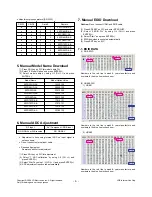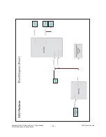
3) HDMI 3
Numbers in the red line is week & year manufacture and
numbers in the blue line is check sum.
4) HDMI 4
Numbers in the red line is week & year manufacture and
numbers in the blue line is check sum.
[
Upper EDID Data used by 60PG30FD-AA model
Caution: It can be different from week & year manufacture and
check sum.
(Because week & year manufacture and check sum is
updated once a year)
ⓐ
Product ID
SET Assembly Adjustment Method
Caution: Each PCB assembly must be checked by check JIG
set.
(Because power PCB Assembly damages to PDP Module,
especially be careful)
Set up “RF mode(noise)” before voltage adjustment.
8. POWER PCB Ass’y Voltage
Adjustment
(Va, Vs Voltage adjustment)
8-1. Test Equipment :
D.M.M. 1EA
8-2.Connection Diagram for Measuring
: refer to Fig.1, Fig.2, Fig.3, Fig.4, Fig.5
8-3. Adjustment Method
(1) 60” Va Adjustment(refer Fig. 1)
1) After receiving 100% Full White Pattern, HEAT RUN.
2) C terminal of D.M.M to Va pin of P811, connect
- terminal to GND pin of P811.
3) After turning VR901, voltage of D.M.M adjustment as
same as Va voltage which on label of panel right/top.
(Deviation; ±0.5V)
(2) 60” Vs Adjustment(refer Fig. 1)
1) C terminal of D.M.M to Vs pin of P811, connect
– terminal to GND pin of P811.
2) After turning VR951, voltage of D.M.M adjustment as
same as Va voltage which on label of panel right/top.
(Deviation; ±0.5V)
(3) 50” Va Adjustment(refer Fig. 2)
1) After receiving 100% Full White Pattern, HEAT RUN.
2) C terminal of D.M.M to Va pin of P811, connect
- terminal to GND pin of P811.
3) After turning VR901, voltage of D.M.M adjustment as
same as Va voltage which on label of panel right/top.
(Deviation; ±0.5V)
- 7 -
Copyright © 2008 LG Electronics. Inc. All right reserved.
Only for training and service purposes
LGE Internal Use Only
a
a
(Fig. 1) 60inch Power PCB Assy Voltage Adjustment


