background image

RS-232C COMMAND(Commonly apply)

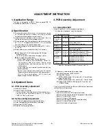
wb 00 00”: Start Auto-adjustment of white balance.

O

“wb 00 10”: Start Gain Adjustment (Inner pattern) 

O

“jb 00 c0” : 

O

O

“wb 00 1f”: End of Adjustment

* If it needs, offset adjustment (wb 00 20-start, wb 00 2f-

end)

O

“wb 00 ff”: End of white balance adjustment (inner
pattern disappear)

Adjustment Mapping information

O

When Color temperature (White balance) Adjustment
(Automatically)

- Press “Power only key” of service remocon and

operate automatically adjustment.

- Set BaudRate to 115200.

O

You must start “wb 00 00” and finish it “wb 00 ff”.

O

If it needs, then adjustment “Offset”.

(4) White Balance Adjustment (Manual adjustment)

1)  Test Equipment: CA-210

- Using PDP color temperature, Color Analyzer (CA-

210) must use CH 10, which Matrix compensated
(White, Red, Green, Blue compensation) with CS-
2100. See the Coordination bellowed one. 

2) Manual adjustment sequence is like bellowed one.

- Turn to “Ez-Adjust” mode with press ADJ button of

service remocon.

- Select “10.Test Pattern” with CH+/- button and press

enter. Then set will go on Heat-run mode. Over 30
minutes set let on Heat-run mode.

- Let CA-210 to zero calibration and must has gap more

10cm from center of PDP module when adjustment. 

- Press “ADJ” button of service remocon and select

“7.White-Balance” in “Ez-Adjust” then press “

G

” button

of navigation key. (When press “

G

” button then set will

go to full white mode)

- Adjust at three mode (Cool, Medium, Warm)
- If “cool” mode 

Let B-Gain to 192 and R, G, B-Cut to 64 and then
control R, G gain adjustment High Light adjustment.

- If “Medium” and “Warm” mode Let R-Gain to 192 and

R, G, B-Cut to 64 and then control G, B gain
adjustment High Light adjustment.

- All of the three mode 

Let R-Gain to 192 and R, G, B-Cut to 64 and then
control G, B gain adjustment High Light adjustment.

- With volume button (+/-) you can adjust.
- After all adjustment finished, with Enter (_ key) turn to

Ez-Adjust mode. Then with ADJ button, exit from
adjustment mode

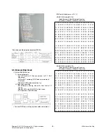
* Attachment: White Balance adjustment coordination and color

temperature.

O

Using CS-1000 Equipment. 

- COOL : T=11000K, _uv=0.000, x=0.276 y=0.283 
- MEDIUM  : T=9300K, _uv=0.000, x=0.285 y=0.293 
- WARM  : T=6500K, _uv=0.000, x=0.313 y=0.329 

O

Using CA-210 Equipment. (10 CH)

- Contras value : 216 Gray

- Brighness spec.

- 10 -

LGE Internal Use Only

Copyright ©2011 LG Electronics Inc. All rights reserved. 
Only for training and service purposes

RS-232C COMMAND

[CMD    ID      DATA]

Meaning

wb

00

00

White Balance adjustment start.

wb

00

10

Start of adjust gain 

(Inner white pattern)

wb

00

1f

End of gain adjust

wb

00

20

Start of offset adjust

(Inner white pattern)

wb

00

2f

End of offset adjust

wb

00

ff

End of White Balance adjust

(Inner pattern disappeared)

RS-232C COMMAND

CENTER

[CMD ID DATA]

MIN

(DEFAULT)

MAX

Cool Mid

Warm

Cool

Mid

Warm

R Gain

jg

Ja

jd

00

184

192

192

192

G Gain

jh

Jb

je

00

187

183

159

192

B Gain

ji

Jc

jf

00

192

161

95

192

R Cut

64

64

64

127

G Cut

64

64

64

127

B Cut

64

64

64

127

Color Test 

Color 

Coordination

temperature

Equipment

x

y

COOL

CA-210

0.276

±

0.002

0.283

±

0.002

MEDIUM

CA-210

0.285

±

0.002

0.293

±

0.002

WARM

CA-210

0.313

±

0.002

0.329

±

0.002

Item

Min

Typ Max Unit

Remark

White  

49

60

-

cd/m - 100%Window White 

average

Pattern

brightness

- 100IRE(255Gray)

- Picture: Vivid(Medium )

Brightness 

-20

+20

%

- 85IRE(216Gray) 100% 

uniformity

Window White Pattern

- Picture: Vivid(Medium)

Summary of Contents for 42PT250B

Page 1: ...TY PRECAUTIONS IN THIS MANUAL CHASSIS PB11K MODEL 50PT490B 50PT490B SA MODEL 50PT490B 50PT490B SD North Latin America http aic lgservice com Europe Africa http eic lgservice com Asia Oceania http biz lgservice com Internal Use Only Printed in Korea P NO MFL66986913 1106 REV00 ...

Page 2: ...right 2011 LG Electronics Inc All rights reserved Only for training and service purposes CONTENTS CONTENTS 2 SAFETY PRECAUTIONS 3 SPECIFICATION 4 ADJUSTMENT INSTRUCTION 6 BLOCK DIAGRAM 13 EXPLODED VIEW 14 SCHEMATIC CIRCUIT DIAGRAM ...

Page 3: ...t s Neck Leakage Current Cold Check Antenna Cold Check With the instrument AC plug removed from AC source connect an electrical jumper across the two AC plug prongs Place the AC switch in the on position connect one lead of ohm meter to the AC plug prongs tied together and touch other ohm meter lead in turn to each exposed metallic parts such as antenna terminals phone jacks etc If the exposed met...

Page 4: ... Power Voltage Standard input voltage 100 V 240 V 50 60 Hz Standard Voltage of each product is marked by models 4 Specification and performance of each parts are followed each drawing and specification by part number in accordance with BOM 5 The receiver must be operated for about 5 minutes prior to the adjustment 3 Test Method 1 Performance LGE TV test method followed 2 Demanded other specificati...

Page 5: ...240V 50 60Hz 4 Market Brazil chile Peru Venezuela PW350B PV550B PT250B PT350B Costarica Uruguay Colombia Panama PW350E PV550E PT250E PT260E 5 Screen Size 42 inch Wide 1024 768 PW350B PW350E PT350B PT250B PT250E PT260E 50 inch Wide 1024 768 PW350B PW350E PT350B PT250B PT250E PT260E 50 inch Wide 1024 768 PV550B PV550E 60 inch Wide 1024 768 PV550B PV550E 6 Aspect Ratio 16 9 50 42PW350B SA 50 42PW350E...

Page 6: ...anufacture Line You can see set adjustment status at 9 ADJUST CHECK of the In start menu 3 2 Set Assembly Adjustment 1 EDID The Extended Display Identification Data 2 Color Temperature White Balance Adjustment 3 Make sure RS 232C control 4 Selection Factory output option 4 PCB Assembly Adjustment 4 1 Using RS 232C Adjust 3 items at 3 1 PCB assembly adjustments 3 Adjustment sequence one after the o...

Page 7: ...ch the signal wait more a second and enter the IN START with press IN START key of Service remocon After then select 7 External ADC with navigator button and press Enter O After Then Press key of Service remocon Right Arrow VOL O You can see ADC Component1 Success O Component1 1080p RGB 1080p Adjust is same method O Component 1080p Adjustment in Component1 input mode O RGB 1080p adjustment in RGB ...

Page 8: ...53 10 00 0A 20 20 20 20 20 20 00 00 00 FC 70 00 4C 47 20 54 56 0A 20 20 20 20 20 20 20 01 0F 0 02 03 27 F1 4E 02 03 11 12 93 04 15 16 05 14 10 10 1F 22 20 26 15 07 50 09 57 07 68 03 0C 00 10 00 20 B8 2D 00 E3 05 03 01 02 3A 80 18 71 38 2D 40 58 30 2C 45 00 40 84 63 00 00 1E 01 1D 80 18 71 1C 16 40 20 58 2C 25 00 40 84 63 00 00 9E 01 1D 00 72 51 50 D0 1E 20 6E 28 55 00 40 84 63 00 00 1E 00 00 00 60...

Page 9: ... Pic 5 O Set Baud Rate of RS 232C to 115200 It may set 115200 orignally O Connect RS 232C cable to set O Connect HDMI cable to set 9 LGE Internal Use Only Copyright 2011 LG Electronics Inc All rights reserved Only for training and service purposes Connection Diagram for Adjustment White balance 0 1 2 3 4 5 6 7 8 9 A B C D E F 0 00 FF FF FF FF FF FF 00 1E 6D 01 00 01 01 01 01 10 01 15 01 03 80 A0 5...

Page 10: ...arm mode Let R Gain to 192 and R G B Cut to 64 and then control G B gain adjustment High Light adjustment All of the three mode Let R Gain to 192 and R G B Cut to 64 and then control G B gain adjustment High Light adjustment With volume button you can adjust After all adjustment finished with Enter _ key turn to Ez Adjust mode Then with ADJ button exit from adjustment mode Attachment White Balance...

Page 11: ...n at 100mA 2 Test time just 1 second 3 Test point GND test Test between Power cord GND and Signal cable metal GND ESD test Test between Power cord GND and Live and neutral 4 Leakage current Set to 0 5mA rms 9 POWER PCB Ass y Voltage Adjustment Va Vs Voltage Adjustment 1 Test equipment D M M 1EA 2 Connection Diagram for Measuring refer to fig 1 9 1 Adjustment method 1 Vs adjustment refer fig 1 1 Co...

Page 12: ... by fixel in 16 9 matrix is applicable 14th 15th fixel in row 3rd 7th fixel in colume And they are numbered from 1 to 10 TV Jig Monitor is numbered samely 4 When checker touched a box numbered 3 of Pen touch TV same box of JIG monitor blinks three times 12 USB DOWNLOAD epk file download V Put the USB Stick to the USB socket V Press Menu key and move OPTION V Press FAV Press 7 times V Select downlo...

Page 13: ... 13 LGE Internal Use Only Copyright 2011 LG Electronics Inc All rights reserved Only for training and service purposes BLOCK DIAGRAM ...

Page 14: ...ated characteristics These parts are identified by in the Schematic Diagram and EXPLODED VIEW It is essential that these special safety parts should be replaced with the same components as recommended in this manual to prevent X RADIATION Shock Fire or other Hazards Do not modify the original design without permission of manufacturer IMPORTANT SAFETY NOTICE LV1 A12 A2 A4 A8 A18 A20 Set Stand Pole ...

Page 15: ...D 15 AD17 PCM_PF_RBZ AA19 UART_TX2 GPIO65 M23 UART_RX2 GPIO64 N23 DDCR_DA GPIO71 M22 DDCR_CK GPIO72 N22 DDCA_DA UART0_TX A5 DDCA_CK UART0_RX B5 PWM0 GPIO66 K23 PWM1 GPIO67 K22 PWM2 GPIO68 G23 PWM3 GPIO69 G22 PWM4 GPIO70 G21 SAR0 GPIO31 C6 SAR1 GPIO32 B6 SAR2 GPIO33 C8 SAR3 GPIO34 C7 SAR4 GPIO35 A6 TCON0 POL N21 TCON2 GSP_R GCLK1 M21 TCON4 CPV GSC GCLK3 L22 TCON6 FLK L21 TCON8 CS2 FLK3 P21 GPIO36 U...

Page 16: ...DD_DA GPIO30 B4 DDCDD_CK GPIO29 C4 HOTPLUGD GPIO22 E5 CEC GPIO5 D6 HSYNC0 G5 VSYNC0 G6 RIN0P K1 RIN0M L3 GIN0P K3 GIN0M K2 BIN0P J3 BIN0M J2 SOGIN0 J1 HSYNC1 G4 VSYNC1 H6 RIN1P K5 RIN1M K4 GIN1P J4 GIN1M K6 BIN1P H4 BIN1M J6 SOGIN1 J5 HSYNC2 H5 RIN2P N3 RIN2M N2 GIN2P M2 GIN2M M1 BIN2P L2 BIN2M L1 SOGIN2 M3 CVBS0P N4 CVBS1P N6 CVBS2P L4 CVBS3P L5 CVBS4P L6 CVBS5P M4 CVBS6P M5 CVBS7P K7 CVBS_OUT1 M...

Page 17: ...7 GND_54 R10 GND_55 R11 GND_56 R12 GND_57 R13 GND_58 R14 GND_59 R15 GND_60 R16 GND_61 R17 GND_62 R18 GND_63 T10 GND_64 T11 GND_65 T12 GND_66 T13 GND_67 T14 GND_68 T15 GND_69 T16 GND_70 T17 GND_71 T18 GND_72 T19 GND_73 U10 GND_74 U11 GND_75 U12 GND_76 U13 GND_77 U14 GND_78 U15 GND_79 U16 GND_80 U17 GND_81 V7 GND_82 V8 GND_83 V9 GND_84 V10 GND_85 V11 GND_86 V12 GND_87 V13 GND_88 V14 GND_89 V15 GND_9...

Page 18: ... AP2121N 3 3TRE1 EAN58801701 1 GND 2 VOUT 3 VIN 5V L509 120 ohm 2A R510 10K R512 1K READY C559 470pF 50V C517 0 01uF 25V C503 10uF 16V 17V C539 0 1uF 16V 5V_TU C520 1000pF JP505 C530 10uF 16V READY C546 100pF 50V R530 0 R505 10K 1 16W 5 C537 10uF 16V L503 3 6uH C505 10uF 16V R507 100 5V_ST_EN C542 0 1uF 50V 3 3V 3 3V_ST R506 100 R502 10K READY R504 10K IC505 1 TJ3964S 2 5 GND VOUT VIN R518 10K Q50...

Page 19: ... 86 RON 87 NC_3 88 HDVDDH 89 NC_4 90 HDVDDL1 91 VSS_11 92 VDDL_7 93 SCKB 94 TEST0 95 SDOB 96 PCKB 97 DENB 98 GPO2 99 VDDH_5 100 AGC_S C682 0 1uF EXTERNAL_DEMOD C692 0 1uF 16V READY C694 0 1uF 16V EXTERNAL_DEMOD C690 0 1uF 16VEXTERNAL_DEMOD IF_N_MSTAR C664 0 1uF EXTERNAL_DEMOD R627 1M EXTERNAL_DEMOD IC600 KIA1117ST00 1 GND ADJ 2 OUT 3 IN C673 0 1uF EXTERNAL_DEMOD C669 0 1uF EXTERNAL_DEMOD C667 0 1u...

Page 20: ...ODE 6 OUT2B 16 CONFIG 15 VDD 14 GND_REG 13 OUT1A 12 GND1 11 VCC1 10 OUT1B 9 OUT2A 8 VCC2 7 GND2 4 VSS 5 VCC_REG 2 SA 21 VDD_DIG_1 1 GND_SUB 20 TWARN OUT4A 19 EAPD OUT4B 18 OUT3A FFX3A 23 PWRDN 24 VDD_PLL 25 FILTER_PLL 22 GND_DIG_1 37 EP GND C728 100uF 25V C713 100uF 25V R702 2 2 R709 0 C7081uF 25V AUD_LRCH R701 2K JP704 C733 22pF 50V READY C723 1000pF 50V R714 22 C711 0 1uF 50V C717 0 22uF 50V C70...

Page 21: ...T24C02BN SH T HDMI2 3 A2 2 A1 4 GND 1 A0 5 SDA 6 SCL 7 WP 8 VCC R843 3 3K HDMI2 3 3V_ST 5V_HDMI_3 R872 0 READY D2 _HDMI4 HPD2 DDC_SDA_3 R871 0 D2 _HDMI2 D807 AVRL161A1R1NT READY DDC_SCL_2 C808 0 1uF 16V HDMI2 R834 18K HDMI1 5V_HDMI_4 Q807 2SC3875S ALY SIDE HDMI E B C 5V_HDMI_3 CEC_REMOTE D2 _HDMI3 D0 _HDMI3 R829 22 HDMI1 3 3V_ST JK804 RSD 105156 100 14 RESERVED 13 CEC 5 TMDS_DATA1_SHIELD 20 BODY_S...

Page 22: ...pF 50V R951 0 232C_NO4 C900 0 1uF 16V EMI_GND4 R953 0 R920 100K USA EDID_WP R952 0 P906 12507WR 03L FOR NON_RGB_DEBUG 1 2 3 4 C915 READY 3 3V_ST R962 0 C905 220pF 50V READY JK901 PEJ027 01 EAG60841801 IR JACK 6B T_TERMINAL2 7B B_TERMINAL2 5 T_SPRING 4 R_SPRING 7A B_TERMINAL1 6A T_TERMINAL1 3 E_SPRING R911 10K C933 10pF LED_WHITE DSUB_R D904 R916 22 R922 0 NON_IR JACK C910 0 1uF 50V R978 22 READY R...

Page 23: ...1094 12K R1003 0 R1075 470K SPDIF_OUT 3 3V COMP1_Y C1005 10pF 50V READY R1096 0 READY C1001 10pF 50V READY R1077 10K COMP1_DET R1095 12K COMP2_Y R1074 75 D1001 5 6V C1011 1000pF 50V COMP2_Pb IC1000 NL17SZ00DFT2G READY 3 GND 2 B 4 Y 1 A 5 VCC COMP2_Pb R1005 0 C1002 10pF 50V READY R1067 75 C1004 10pF 50V READY AV_CVBS_DET R1038 470K R1080 1K D1020 30V COMP1_Pr R1079 470K R1098 0 READY D1010 5 6V R10...

Page 24: ... 3AU04S 305 ZC LG 1 2 3 4 5 IC1101 AP2191SG 13 SIDE USB 3 IN_2 2 IN_1 4 EN 1 GND 5 FLG 6 OUT_1 7 OUT_2 8 NC 5V C1122 10uF 16V SIDE USB USB1_DP_to_MAIN USB1_CTL C1121 0 1uF 16V SVC USB USB2_DM_to_MAIN 3 3V 5V USB1_OCD L1100 MLB 201209 0120P N2 0LCML00003B SVC USB R1141 10K READY C1120 0 1uF 16V SIDE USB USB2_DP_to_MAIN D1102 5 6V CDS3C05HDMI1 READY JK1100 KJA UB 0 0037 SVC USB 1 2 3 4 5 D1103 5 6V ...

Page 25: ...DD_5 K8 VDD_6 N1 VDD_7 N9 VDD_8 R1 VDD_9 R9 VDDQ_1 A1 VDDQ_2 A8 VDDQ_3 C1 VDDQ_4 C9 VDDQ_5 D2 VDDQ_6 E9 VDDQ_7 F1 VDDQ_8 H2 VDDQ_9 H9 NC_1 J1 NC_2 J9 NC_3 L1 NC_4 L9 NC_6 T7 VSS_1 A9 VSS_2 B3 VSS_3 E1 VSS_4 G8 VSS_5 J2 VSS_6 J8 VSS_7 M1 VSS_8 M9 VSS_9 P1 VSS_10 P9 VSS_11 T1 VSS_12 T9 VSSQ_1 B1 VSSQ_2 B9 VSSQ_3 D1 VSSQ_4 D8 VSSQ_5 E2 VSSQ_6 E8 VSSQ_7 F9 VSSQ_8 G1 VSSQ_9 G9 A TMA12 B TMDQU2 A TMDQL2...

Page 26: ... E B C R1322 1K EXTERNAL_DEMOD R1343 10K TU_2INPUT_CTRL C1325 100pF 50V R1300 3K C1311 0 01uF 25V TU_2INPUT_CTRL R1334 0 3 3V 5V_TU C1312 62pF 50V L1303 MLB 201209 0120P N2 TU_2INPUT_CTRL Q1305 ISA1530AC1 E B C TUNER_RESET 5V_TU C1306 0 1uF R1323 1K INTERNAL_DEMOD C1317 0 1uF 16V INTERNAL_DEMOD R1325 4 7K C1301 100uF 16V 3 3V R1329 470 TU_SCL 5V_TU R1324 0 READY L1305 270nH R1330 220 TU1300 1 UDA5...

Page 27: ...A_1_E C1481 0 1uF 16V LVDS_DATA_2_E 5V DDR2_CLK DDR_DQS1M TE1P DISP_EN R1553 0 R1417 22 DDR_CS R1468 100 LVDS_CLK_2 C1490 0 1uF 16V DDR_DQS0P C1528 1000pF READY IC1406 AZ1085S 3 3TR E1 1 ADJ GND 2 OUTPUT 3 INPUT R1574 0 READY TC2P C1535 4 7uF 10V READY TD1N R1521 0 R1532 0 TD4N R1561 0 C1516 0 1uF 16V TB4P R1481 3 3K P1403 12507WS 04L READY 1 2 3 4 5 R1546 0 TCLK2N R1495 3 3K 3D_ASIC 3D_L R_SYNC_F...

Page 28: ......
Page 29: ...ATSC Group GP2 R Team Great Company Great People GP2 R Training manual GP2 R Training manual Contents Block Diagram System Design Trouble Shooting Guide ...

Page 30: ...al Flash DDR3 IF COMP1 COMP2 Y Cb Cr Y Cb Cr R G B RGB PC Rear AV CVBS Side AV CVBS AV1 2 L R COMP 1 2 L R L R L R HDMI 1 HDMI 2 HDMI 3 TMDS DDC TMDS DDC Video Front End Audio Front End HDMI RX LVDS out HD WXGA XGA FHD 2D 3D HD SD Video Encoder STA368 Digital AMP I2S MCLK Audio DSP SPDIF Out UART RX TX DDC SIF Cable ISDB T PAL NTSC Rear USB SVC only Side USB USB2 0 LVDS Con HD FHD 3D LVDS Con HD F...

Page 31: ...F1 Cable ISDB T PAL NTSC System Scalar IF I2S TAS5709 TAS5709 AV1 AV1_LR COMP1_LR COMP2_LR RGB_LR EXT_IN AV2 AV2_LR NANDFlash 256MB NANDFlash 256MB Audio Out USB2 0 SPDIF SIF_LIVE I2S_BCM Comp1 2 RGB HDMI_Rear D port HDMI_Side C port SIDE HDMI_PORT UI_HW_PORT1 HDMI_C Demodulator MN884433 TP1 Serial_Flash 1MB Serial_Flash 1MB USB Rear USB SVC only Side USB 1 Power Up Boot Fail Trouble Shooting Rear...

Page 32: ...s Inc All rights reserved Only for training and service purposes LGE Internal Use Only Reset Design TAS5709 AMP Demodulator GPIO Reset Active Low S7 Main Soc H W Reset Active High Tuner GPIO Reset Active Low GPIO Reset Active Low ...

Page 33: ...ernal Use Only S7 Power Sequence Appendix Power Up Sequence Time Power XTAL 3 3V AVDD_DMPLL Reset HI Active 1 5V 1 8V with Other Power 1 26V t1 t3 3 3V VDDP t4 t2 Note 3 3V_AVDD_MPLL AVDD_DMPLL 1 05V VDDC 3 3V_VDDP VDDP 1 5V 1 8V AVDD_DDR0 1 Other Power AVDD_AU25 AVDD_AU33 AVDD_MEMPLL AVDD2P5_ADC etc ...

Page 34: ...aining and service purposes LGE Internal Use Only S7 Power Sequence Appendix Time Description Min Typ Max Unit t1 XTAL stable to Reset falling 5 ms t2 Reset pulse width 5 ms t3 1 26V to Reset falling 5 ms t4 3 3VDDP to Reset falling 5 ms Power Up Timing Requirements ...

Page 35: ...Copyright 2011 LG Electronics Inc All rights reserved Only for training and service purposes LGE Internal Use Only S7 Power Sequence t2 Reset Pulse Width 40ms Æ OK ...

Page 36: ...l Use Only a AC On b DC Remocon On 1 X tal 2 3 3V 3 1 26V 4 Reset S7 Power Sequence 1 X tal 2 3 3V 3 1 26V 4 Reset t1 Reset Pulse Width 400ms Æ OK t3 Reset Pulse Width 400ms Æ OK t4 Reset Pulse Width 400ms Æ OK t1 Reset Pulse Width 120ms Æ OK t3 Reset Pulse Width 120ms Æ OK t4 Reset Pulse Width 120ms Æ OK ...

Page 37: ...DEMOD BRAZIL MN884433 0xD8 CH 2 PDP MODULE 0x1C PDP MODULE 0x1C CH 5 DDCDB_CK GPIO25 DDCDB_DA GPIO26 EEPROM HDMI1 0XA0 EEPROM HDMI1 0XA0 DDCDD_CK GPIO29 B4 C4 DDC_SCL3 DDC_SDA3 5V_HDMI_2 5 0V DDCDD_DA GPIO30 CH 12 EEPROM HDMI1 0XA0 EEPROM HDMI1 0XA0 DDCDC_CK GPIO27 AA4 AB4 DDC_SCL4 DDC_SDA4 5V_HDMI_Side 5 0V DDCDC_DA GPIO28 CH 11 EEPROM RGB 0XA0 EEPROM RGB 0XA0 DDCA_CK UART0_RX N22 M22 RGB_DDC_SCL...

Page 38: ...ut USB1_OCD 5 Module Rom download UART Output MOD_ROM_TX 51 Compnent1 Auto link Input COMP1_DET 40 HDMI_1 5V Detect Input 5V_DET_HDMI_3 TCON6 FLK HDMI Side 5V Detect Input 5V_DET_HDMI_4 TCON4 CPV GSC_R G CLK3 HDMI3 Ready HDMI 5V Detect Input 5V_DET_HDMI_2 TCON2 GSP _R GCLK1 Model option 2 RF_SWITCH_CTL Input Output Model_OPT_2 14 Model option 1 FE_BOOSTER_CTRL Input Output Model_OPT_1 11 Model opt...

Page 39: ...R201 IC602 MN884433 L609 3 3V 3 3V 3 3V 3 3V 3 3V_DE IC600 AZ1117 1 2V_DE IC801 802 804 HDMI eeprom CEC FET BSS83 IC901 RGB eeprom P904 3D LVDS IC900 MAX3232 P905 Emitter board P905 Emitter board L900 L901 IC1101 AP21915 USB SVC IC1000 NAND gate IC1201 2 DDR3 5 65 L1201 TU1300 Tuner 1 2V_DE L1301 3 3V L1300 L1303 1 05V_VDDC L323 VDDC 1 05V_VDDC L321 1 05V_MIU1VDDC 1 05V_VDDC L324 1 05V_MIU0VDDC L3...

Page 40: ...Trouble Shooting 5 Component Video Trouble Shooting 6 RGB Video Trouble Shooting 7 AV Video Trouble Shooting 8 HDMI Video Trouble Shooting 9 All Source Audio Trouble Shooting 10 Digital TV Audio Trouble Shooting 11 Analog TV Audio Trouble Shooting 12 Component RGB AV Audio Trouble Shooting 13 HDMI Audio Trouble Shooting 14 USB Trouble Shooting Trouble Shooting Guide for LG Service Man Please check...

Page 41: ...BCM TAS9709 TAS9709 AV1 AV1_LR COMP1_LR COMP2_LR RGB_LR EXT_IN AV2 AV2_LR NANDFlash 256MB NANDFlash 256MB Audio Out USB2 0 SPDIF SIF_LIVE I2S_BCM Comp1 2 RGB HDMI_Rear D port HDMI_Side C port SIDE HDMI_PORT UI_HW_PORT1 HDMI_C Demodulator MN884433 TP1 Serial_Flash 1MB Serial_Flash 1MB USB Rear USB SVC only PJ230 Side USB 1 Power Up Boot Fail Trouble Shooting Reset HDMI CEC Stand by IR I2C KIA7427AF...

Page 42: ... voltage level 3 3V RL_ON Replace one of IC501 Recheck N Y Check Voltage Level 1 5V at IC502 7 pin N Check R500 voltage level ON OFF Control Replace one of IC502 Recheck N Y Check Voltage Level 2 5V at C589 N Replace one of IC505 and application circuit Recheck N Y Check X200 Clock24MHz N Replace X200 Y Check signal transition at IC103 N Maybe Serial Flash Memory problem Check signal transition IC...

Page 43: ...F I2S_BCM TAS9709 TAS9709 AV1 AV1_LR COMP1_LR COMP2_LR RGB_LR EXT_IN AV2 AV2_LR NANDFlash 256MB NANDFlash 256MB Audio Out USB2 0 SPDIF SIF_LIVE I2S_BCM Comp1 2 RGB HDMI_Rear D port HDMI_Side C port SIDE HDMI_PORT UI_HW_PORT1 HDMI_C Demodulator MN884433 TP1 Serial_Flash 1MB Serial_Flash 1MB USB Rear USB SVC only PJ230 Side USB Reset HDMI CEC Stand by IR I2C KIA7427AF KIA7427AF 24C16 24C16 Local Loc...

Page 44: ...at Q501 N Replace one of Q501 Recheck Y Check P903 TXAC TXAC TXBC TXBC Display Enable N Y Check LVDS Cable N Replace Cable Y Check PDP Module Check 5V Voltage Level at L507 L501 N Replace one of L507 501 Recheck Y Maybe S7 IC101 has troubles It should satisfy the Pixel Clock on CAS Electrical Specifications Power Supply Sequence Input Signal Timing Specification Control Signal Register Check CAS C...

Page 45: ...sing edge when Power On Td_on msec 6000 1500 Time interval between DISPEN falling edge and 90 of Vs when Power Off Td_off Recommended 2sec msec 300 10 Rising Time of Va 10 to 90 TVaR msec 400 100 Rising Time of Vs 10 to 90 TVsR msec 500 50 Falling Time of Va 90 to 10 TVaF msec 20 Time interval between 10 of Vs and 90 of Vcc when Power Off TOff msec 1250 750 Time interval between 90 of Vcc and 10 o...

Page 46: ...K Check SCL SDA line Check Signal output N Y SCL continue SDA continue ACK By Slave 9 1 D0 D7 9 ACK By Slave Command Data for Addr Stop By Master D6 SCL 8 SDA 0 0 1 1 1 A7 W Start By Master Chip ID Address Byte 0x1C ACK By Slave 0 1 9 1 A6 A1 A0 Command Address Addr A 7 0 0 Write only Master Image Board Slave PDP Module Sample Signal SCL SDA ACK signal Check Low OK High Error Replace Control Board...

Page 47: ..._BCM TAS9709 TAS9709 AV1 AV1_LR COMP1_LR COMP2_LR RGB_LR EXT_IN AV2 AV2_LR NANDFlash 256MB NANDFlash 256MB Audio Out USB2 0 SPDIF SIF_LIVE I2S_BCM Comp1 2 RGB HDMI_Rear D port HDMI_Side C port SIDE HDMI_PORT UI_HW_PORT1 HDMI_C Demodulator MN884433 TP1 Serial_Flash 1MB Serial_Flash 1MB USB Rear USB SVC only PJ230 Side USB Reset HDMI CEC Stand by IR I2C KIA7427AF KIA7427AF 24C16 24C16 Local Local KE...

Page 48: ...F Cable Y Check TP Clock Data Sync R630 R631 R632 N Maybe Demodulator has problems Y Maybe MstarS7 IC100 has problems Check Tuner TU1300 Power 5 0V 3 3V 1 2V N Replace one of Bead Recheck Y Check IF Signal pin 17 18 N Maybe Tuner has problems Y Check Demodulator Power 3 3V 1 2V L609 IC600 N Replace L609 IC600 Y Check Demodulator X TAL X602 N Replace X TAL Y ...

Page 49: ..._BCM TAS9709 TAS9709 AV1 AV1_LR COMP1_LR COMP2_LR RGB_LR EXT_IN AV2 AV2_LR NANDFlash 256MB NANDFlash 256MB Audio Out USB2 0 SPDIF SIF_LIVE I2S_BCM Comp1 2 RGB HDMI_Rear D port HDMI_Side C port SIDE HDMI_PORT UI_HW_PORT1 HDMI_C Demodulator MN884433 TP1 Serial_Flash 1MB Serial_Flash 1MB USB Rear USB SVC only PJ230 Side USB Reset HDMI CEC Stand by IR I2C KIA7427AF KIA7427AF 24C16 24C16 Local Local KE...

Page 50: ...e Only 4 Analog TV Video Trouble Shooting Check RF Cable Y Check CVBS Signal TU1300 11 Pin N Y Check CVBS Signal R1334 N Replace one of R1330 Q1305 R154 C213 Recheck Y N Y Check Tuner Power 5 0V 3 3V 1 2V Replace one of L1301 L1300 L1302 Recheck Maybe Tuner TU1300 has problems Maybe MstarS7 IC100 has problems ...

Page 51: ..._BCM TAS9709 TAS9709 AV1 AV1_LR COMP1_LR COMP2_LR RGB_LR EXT_IN AV2 AV2_LR NANDFlash 256MB NANDFlash 256MB Audio Out USB2 0 SPDIF SIF_LIVE I2S_BCM Comp1 2 RGB HDMI_Rear D port HDMI_Side C port SIDE HDMI_PORT UI_HW_PORT1 HDMI_C Demodulator MN884433 TP1 Serial_Flash 1MB Serial_Flash 1MB USB Rear USB SVC only PJ230 Side USB Reset HDMI CEC Stand by IR I2C KIA7427AF KIA7427AF 24C16 24C16 Local Local KE...

Page 52: ...ooting Check Signal Format Is it supported signal Y Check Component Jack JK1001 N Y Check Component Signal R1020 R1021 R1022 R1005 R1012 R1013 N Replace one of R1020 R1021 R1022 R1005 R1012 R1013 Recheck Y Check Component Signal R175 R173 R177 R180 R182 R184 N Replace it Y Y Check Component Cable Replace Jack Maybe Mstar S7 IC100 has problems ...

Page 53: ...I2S_BCM TAS9709 TAS9709 AV1 AV1_LR COMP1_LR COMP2_LR RGB_LR EXT_IN AV2 AV2_LR NANDFlash 256MB NANDFlash 256MB Audio Out USB2 0 SPDIF SIF_LIVE I2S_BCM Comp1 2 RGB HDMI_Rear D port HDMI_Side C port SIDE HDMI_PORT UI_HW_PORT1 HDMI_C Demodulator MN884433 TP1 Serial_Flash 1MB Serial_Flash 1MB USB Rear USB SVC only PJ230 Side USB Reset HDMI CEC Stand by IR I2C KIA7427AF KIA7427AF 24C16 24C16 Local Local...

Page 54: ...B Video Trouble Shooting Check Signal Format Is it supported signal Y Check RGB Jack P901 N Y Y Check RGB Cable Replace Jack Check RGB Signal R907 R908 R909 N Replace It Recheck Y Check Sync Signal N Replace one of R915 R916 Recheck Y Check EEPROM IC901 N Replace it or re burn Recheck Y Maybe Mstar S7 IC101 has problems ...

Page 55: ... I2S_BCM TAS9709 TAS9709 AV1 AV1_LR COMP1_LR COMP2_LR RGB_LR EXT_IN AV2 AV2_LR NANDFlash 256MB NANDFlash 256MB Audio Out USB2 0 SPDIF SIF_LIVE I2S_BCM Comp1 2 RGB HDMI_Rear D port HDMI_Side C port SIDE HDMI_PORT UI_HW_PORT1 HDMI_C Demodulator MN884433 TP1 Serial_Flash 1MB Serial_Flash 1MB USB Rear USB SVC only PJ230 Side USB Reset HDMI CEC Stand by IR I2C KIA7427AF KIA7427AF 24C16 24C16 Local Loca...

Page 56: ... AV Video Trouble Shooting Y Check Jack JK1001 JK1002 N Y Check CVBS Signal C1016 C1018 N Y Check CVBS Signal R187 R188 C226 C227 N Replace one of R187 R188 C226 C227 Recheck Y Y Replace Jack Maybe Mstar S7 IC101 has problems Check Signal Format Is it supported signal Check AV Cable Replace one of C1016 C1018 Recheck ...

Page 57: ...I2S_BCM TAS9709 TAS9709 AV1 AV1_LR COMP1_LR COMP2_LR RGB_LR EXT_IN AV2 AV2_LR NANDFlash 256MB NANDFlash 256MB Audio Out USB2 0 SPDIF SIF_LIVE I2S_BCM Comp1 2 RGB HDMI_Rear D port HDMI_Side C port SIDE HDMI_PORT UI_HW_PORT1 HDMI_C Demodulator MN884433 TP1 Serial_Flash 1MB Serial_Flash 1MB USB Rear USB SVC only PJ230 Side USB Reset HDMI CEC Stand by IR I2C KIA7427AF KIA7427AF 24C16 24C16 Local Local...

Page 58: ... purposes LGE Internal Use Only 8 HDMI Video Trouble Shooting Check Signal Format Is it supported signal Y Check HDMI Jack JK803 JK804 N Y Y Check HDMI Cable Replace Jack Check I2C Signal R844 R845 R858 R859 R848 R849 R862 R863 N Replace It Recheck Y Maybe Mstar S7 IC101 has problems ...

Page 59: ...S_S7 TAS9709 TAS9709 AV1 AV1_LR COMP1_LR COMP2_LR RGB_LR EXT_IN AV2 AV2_LR NANDFlash 256MB NANDFlash 256MB Audio Out USB2 0 SPDIF SIF_LIVE I2S_S7 Comp1 2 RGB HDMI_Rear D port HDMI_Side C port SIDE HDMI_PORT UI_HW_PORT1 HDMI_C Demodulator MN884433 TP1 Serial_Flash 1MB Serial_Flash 1MB USB Rear USB SVC only PJ230 Side USB Reset HDMI CEC Stand by IR I2C KIA7427AF KIA7427AF 24C16 24C16 Local Local KEY...

Page 60: ...can t hear any audio Y Check Connector P703 N Y Y Check Speaker Replace Connector Check Signal L700 L701 N Replace one of Capacitor Register Recheck Y Check IC700 Power 17V 3 3V L702 L703 N Replace It Recheck Y Check Mstar S7 I2S Output R724 R725 R726 N Replace It Recheck Y Maybe Mstar S7 IC101 has problems Replace Speaker N N Maybe TAS9709 has problems Replace It ...

Page 61: ...BCM TAS9709 TAS9709 AV1 AV1_LR COMP1_LR COMP2_LR RGB_LR EXT_IN AV2 AV2_LR NANDFlash 256MB NANDFlash 256MB Audio Out USB2 0 SPDIF SIF_LIVE I2S_BCM Comp1 2 RGB HDMI_Rear D port HDMI_Side C port SIDE HDMI_PORT UI_HW_PORT1 HDMI_C Demodulator MN884433 TP1 Serial_Flash 1MB Serial_Flash 1MB USB Rear USB SVC only PJ230 Side USB Reset HDMI CEC Stand by IR I2C KIA7427AF KIA7427AF 24C16 24C16 Local Local KEY...

Page 62: ...ning and service purposes LGE Internal Use Only 10 Digital TV Audio Trouble Shooting Check video output Y Follow procedure All source audio trouble shooting Maybe Mster S7 internal audio DSP has problems Replace It N Follow procedure digital TV video trouble shooting N ...

Page 63: ..._BCM TAS9709 TAS9709 AV1 AV1_LR COMP1_LR COMP2_LR RGB_LR EXT_IN AV2 AV2_LR NANDFlash 256MB NANDFlash 256MB Audio Out USB2 0 SPDIF SIF_LIVE I2S_BCM Comp1 2 RGB HDMI_Rear D port HDMI_Side C port SIDE HDMI_PORT UI_HW_PORT1 HDMI_C Demodulator MN884433 TP1 Serial_Flash 1MB Serial_Flash 1MB USB Rear USB SVC only PJ230 Side USB Reset HDMI CEC Stand by IR I2C KIA7427AF KIA7427AF 24C16 24C16 Local Local KE...

Page 64: ...ing N Check video output Y Check SIF Signal TU1300 9 Pin N Y N Y Follow procedure All source audio trouble shooting N Maybe Mstar S7 audio block has problems Replace It N Y Check Tuner Power 5 0V 3 3V 1 2V Replace one of L1300 L1301 L1302 Recheck Maybe Tuner TU1300 has problems Replace one of C252 R246 R1332 Q1304 R1325 IC501 Recheck Check SIF Signal SIF waveform sample Defend on the input signal ...

Page 65: ... TAS9709 TAS9709 AV1 AV1_LR COMP1_LR COMP2_LR RGB_LR EXT_IN AV2 AV2_LR NANDFlash 256MB NANDFlash 256MB Audio Out USB2 0 SPDIF SIF_LIVE I2S_BCM Comp1 2 RGB HDMI_Rear D port HDMI_Side C port SIDE HDMI_PORT UI_HW_PORT1 HDMI_C Demodulator MN884433 TP1 Serial_Flash 1MB Serial_Flash 1MB USB Rear USB SVC only PJ230 Side USB Reset HDMI CEC Stand by IR I2C KIA7427AF KIA7427AF 24C16 24C16 Local Local KEY KE...

Page 66: ...C205 R166 R167 R168 R169 R170 R171 R127 C215 C216 C203 C217 C218 C219 C204 R187 R188 C226 C227 N Replace Jack Check Video Output Replace one of C206 C207 C208 C209 C210 C211 C212 C220 C221 C222 C223 C224 C225 C205 R166 R167 R168 R169 R170 R171 R127 C215 C216 C203 C217 C218 C219 C204 R187 R188 C226 C227 Recheck N Follow procedure external input video trouble shooting Y Follow procedure All source a...

Page 67: ...2S_BCM TAS9709 TAS9709 AV1 AV1_LR COMP1_LR COMP2_LR RGB_LR EXT_IN AV2 AV2_LR NANDFlash 256MB NANDFlash 256MB Audio Out USB2 0 SPDIF SIF_LIVE I2S_BCM Comp1 2 RGB HDMI_Rear D port HDMI_Side C port SIDE HDMI_PORT UI_HW_PORT1 HDMI_C Demodulator MN884433 TP1 Serial_Flash 1MB Serial_Flash 1MB USB Rear USB SVC only PJ230 Side USB Reset HDMI CEC Stand by IR I2C KIA7427AF KIA7427AF 24C16 24C16 Local Local ...

Page 68: ...ce purposes LGE Internal Use Only 13 HDMI Audio Trouble Shooting Check video output Y Follow procedure All source audio trouble shooting N Y Re download EDID data Maybe Mstar S7 audio block has problems Replace it N Follow procedure HDMI video trouble shooting N Replace IC802 IC804 ...

Page 69: ...IF I2S_BCM TAS9709 TAS9709 AV1 AV1_LR COMP1_LR COMP2_LR RGB_LR EXT_IN AV2 AV2_LR NANDFlash 256MB NANDFlash 256MB Audio Out USB2 0 SPDIF SIF_LIVE I2S_BCM Comp1 2 RGB HDMI_Rear D port HDMI_Side C port SIDE HDMI_PORT UI_HW_PORT1 HDMI_C Demodulator MN884433 TP1 Serial_Flash 1MB Serial_Flash 1MB USB Rear USB SVC only PJ230 Side USB Reset HDMI CEC Stand by IR I2C KIA7427AF KIA7427AF 24C16 24C16 Local Lo...

Page 70: ...y inrushing current In this case remove the device and try to reboot the TV AC power off on Check USB 2 0 Cable Y Check P1102 250 350 tool P1100 230 tool N Y Y Check USB device If device is 2 5 inch HDD Check power adaptor Replace Jack Check 5V voltage level IC1101 2 250 350 tool L1100 230 tool N Replace one of IC1101 L1100 Recheck Y MaybeMstar S7 IC101 has problems Replace It ...

Reviews: