background image

- 27 -

LGE Internal Use Only

Copyright©2008 LG Electronics. Inc. All right reserved. 
Only for training and service purposes

EXPLODED VIEW

603

602

601

520

400

590

501

307

120

121

306

560

570

571

310

302

303

305

300

304

200

250

901

900

240

209

208

201

204

207

A2

205

206

580

202

203

301

Many electrical and mechanical parts in this chassis have special safety-related characteristics. These
parts are identified by       in the Schematic Diagram and EXPLODED VIEW. 
It is essential that these special safety parts should be replaced with the same components as
recommended in this manual to prevent X-RADIATION, Shock, Fire, or other Hazards. 
Do not modify the original design without permission of manufacturer.

IMPORTANT SAFETY NOTICE

Summary of Contents for 42PG20D-DA

Page 1: ...V SERVICE MANUAL CAUTION BEFORE SERVICING THE CHASSIS READ THE SAFETY PRECAUTIONS IN THIS MANUAL CHASSIS PT81A MODEL 50PG60UD 50PG60UD DA website http biz LGservice com Internal Use Only CH VOL MENU INPUT ENTER ...

Page 2: ...ht 2008 LG Electronics Inc All right reserved Only for training and service purposes CONTENTS CONTENTS 2 SAFETY PRECAUTIONS 3 SPECIFICATION 4 ADJUSTMENT INSTRUCTION 6 TROUBLE SHOOTING 11 BLOCK DIAGRAM 20 EXPLODED VIEW 27 SVC SHEET 29 ...

Page 3: ...n handling the Picture Tube Do not lift the Picture tube by it s Neck Leakage Current Cold Check Antenna Cold Check With the instrument AC plug removed from AC source connect an electrical jumper across the two AC plug prongs Place the AC switch in the on position connect one lead of ohm meter to the AC plug prongs tied together and touch other ohm meter lead in turn to each exposed metallic parts...

Page 4: ... drawing and specification by part number in accordance with SBOM 5 The receiver must be operated for about 20 minutes prior to the adjustment V Test Method 1 Performance LGE TV test method followed 2 Demanded other specification Safety CE IEC specification EMC CE IEC V General Specification XGA Module Display Screen Device Aspect Ratio PDP Module Operating Environment Storage Environment Input Vo...

Page 5: ... MNT Out 1EA Video Input 2EA S Video Input 1EA Component Input 2EA RGB Input 1EA HDMI Input 2EA Audio Input 6EA 1 2 3 4 5 6 7 8 9 10 No Item Specification Remark Taiwan Analog NTSC M DTV DVB T 1 VHF 2 13 2 UHF 14 69 3 CATV 1 14 125 4 DTV 14 69 NTSC NTSC NTSC Y Cb Cr Y Pb Pr RGB PC HDMI DTV SOUND PC Audio Component AV Rear 1 Rear 1 Side 1 Side 1 60Hz Only 60Hz Only 60Hz Only L R Input ...

Page 6: ...ignal generator in this mode Single color pattern RED BLUE GREEN of HEAT RUN mode uses to check PANEL Caution If you turn on a still screen more than 20 minutes Especially digital attern cross hatch pattern an after image may be occur in the black level part of the screen 3 S W auto download using the USB Memory stick 1 Insert the USB memory sick the PCB ASSEMBLY 2 Using power on button of the con...

Page 7: ...NTER V 4 EDID download is executed automatically 5 Press EXIT key on R C 7 2 EDID DATA 1 HDMI1 256bytes 2 RGB 128bytes Detail EDID Options below Product ID Serial No Conntrolled on producion line Month Year Conntrolled on producion line Model Name Checksum Changeable by total EDID data 8 PCMCIA CARD Checking Method You must adjust DTV 29 Channel and insert PCMCIA CARD to socket 1 If PCMCIA CARD wo...

Page 8: ...nel 10 which is Matrix compensated White Red Green Blue revised by CS 1000 and adjust in accordance with balance adjustment coordinate W Color temperature standards according to CSM and Module W Change target luminance and range of the Auto adjustment W B equipment W White balance adjustment coordinate and color temperature PC for communication through RS 232C UART Baud rate 115200 bps Each PCB as...

Page 9: ...k the sensor to the center of PDP module 3 Press ADJ KEY on R C and enter EZ ADJUST Select 2 White Balance and press G VOL Set test pattern on and display inside pattern 5 Control is carried out on three color temperatures COOL MEDIUM WARM Control is carried out thress times Temperature COOL R Cut G Cut B Cut is set to 64 Control R Gain and G Gain Each Gain is limited to 192 Temperature MEDIUM R C...

Page 10: ...t remote controller before the factory shipment 1 2 3 4 5 6 7 8 9 Antenna 10 Off 16 9 1 Vivid Medium Off Auto Standard Off 0 On On Off On Off Normal Level 0 Item Condition No Remark Input Mode Volume Level Mute Aspect Ratio SET ID Picture PSM Color Temp Advanced Cinema Black level Sound SSM AVL Balance TV Speaker Time Auto Clock Manual Clock Off Timer On Timer Sleep Timer Auto Off Option SIMPLINK ...

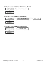
Page 11: ...Monitor signal come out Yes 7 Check the VSC Vs ON signal Doesn t the high tension output come out Doesn t the VSC signal Vs ON come out Yes Yes Does high tension output voltage Drop occur When the Y B D Module input connector is removed does output voltage drop occur When the Y Z B D Module input connector is remove does Power Board hightension output voltage Drop occur Yes No No 9 Check the Power...

Page 12: ...2 AC INLET PDP MODULE AC NC AC YH396 03P Vs Vs NC GND GND Va Va GND M5V M5V YH396 10P Vs Vs NC GND GND Va Va GND M5V M5V YH396 10P 1 2 3 4 5 6 7 8 9 10 Wafer P N NO P21 SMW200 22C VSC BOARD 1 2 3 4 5 6 7 8 9 10 11 12 13 14 15 16 17 18 19 20 21 22 Wafer P N 16V GND 12V GND 5V 5V GND GND 5V_MNT RL_ON M5V_ON 16V GND 12V GND 5V 5V GND GND AC_DET VaVs_ON GND NO 2 Pin Spec ...

Page 13: ... 2 Check following A Power cord is plugged with TV set Plug the power cord Yes No Is the AC INLET connected with the power board Connect the AC INLET Yes No Is the Fuse F101 F801 on Power Board normal Replace the Fuses Yes No Is the Power Board with VSC Board though Cable connected Connect the Cable Yes No Measure output voltages 16V 12V 5V on the power board If the measured values is not normal r...

Page 14: ... of Ctrl B D Yes No Yes Is the Y Board normal Is the output voltage normal after remove P209 connector of Y B D Is the Fuse FS201 on Y B D normal In case of open is replace Yes No Yes Yes Replace Z Board Is the Z Board normal Is the output voltage normal after remove P3 connector of Z B D Is the Fuse FS1 on Z B D normal In case of open is replace Yes No Yes Is the X Board normal Is the output volt...

Page 15: ...ormal Is the VAVS on Check the PDP Module Yes No YES Yes Reconnect the LVDS cable in P501 No Is the IC700 FLI106X0H Output normal Replace the VSC No NO Replace the Power board Is output the normality Low High voltage except stand by 5V NO 4 No Raster 1 Symptom 1 No OSD and image occur at screen 2 It maintains the condition where the front LED is green 2 Check following ...

Page 16: ...Symptom 1 LED is green 2 The minute discharged continuously becomes Accomplished from module 2 Check following Is the LVDS cable normal Is the VSC Board normal Is the LVDS cable connected Connect the LVDS cabel with the VSC board Yes No No Yes Is the IC100 FLI106X0H normal Replace the IC100 FLI106X0H No Is the Ctrl Board of Module normal Replace the Ctrl B D No No Yes Replace the VSC B D Replace t...

Page 17: ...ality display 3 In case of becomes unusual display from RF mode 4 In the case of becomes unusual display from side S video AV mod Is the Tuner normal Is the RF cable connected with TV Set Connect the RF cable Yes No No Is the IC100 FLI106X0H normal Replace the Tuner TU301 No Is the Input voltage IIC Communication and CVBS output normal Yes Is the IIC communication waveform between the tuner and IC...

Page 18: ...ecomes unusual display from HDMI mode 7 In the case of becomes unusual display from SCART mode Is the R G B input and H V Sync of the JK104 normal Check the input source No Is the HDMI IC201 normal Yes Same as Block A Is the TMDS waveform between the IC and HDMI jacks normal No Is the Video input of AV jack normal Yes Same as Block A Check the input source No Replace the IC201 No Yes Same as Block...

Page 19: ...2 Check following All input mode is no sound Only HDMI is No Sound Yes Download the EDID data Yes No YES Only RF is no sound Check the Tuner s IN OUTPUT Yes No Is the IC629 normal Replace the IC629 MSP4458 No Is the IC601 normal Replace the IC601 NTP 3000A No YES Replace the VSC Board YES Is the speakers turned on Set on the speakers on menu No Is the speaker Cable connect Connect the Speaker Cabl...

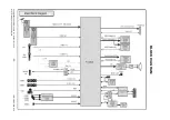
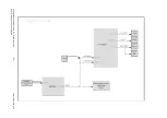
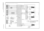
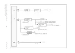
Page 20: ... 20 LGE Internal Use Only Copyright 2008 LG Electronics Inc All right reserved Only for training and service purposes BLOCK DIAGRAM ...

Page 21: ... 21 LGE Internal Use Only Copyright 2008 LG Electronics Inc All right reserved Only for training and service purposes ...

Page 22: ... 22 LGE Internal Use Only Copyright 2008 LG Electronics Inc All right reserved Only for training and service purposes ...

Page 23: ... 23 LGE Internal Use Only Copyright 2008 LG Electronics Inc All right reserved Only for training and service purposes ...

Page 24: ... 24 LGE Internal Use Only Copyright 2008 LG Electronics Inc All right reserved Only for training and service purposes ...

Page 25: ... 25 LGE Internal Use Only Copyright 2008 LG Electronics Inc All right reserved Only for training and service purposes ...

Page 26: ... 26 LGE Internal Use Only Copyright 2008 LG Electronics Inc All right reserved Only for training and service purposes ...

Page 27: ...05 206 580 202 203 301 Many electrical and mechanical parts in this chassis have special safety related characteristics These parts are identified by in the Schematic Diagram and EXPLODED VIEW It is essential that these special safety parts should be replaced with the same components as recommended in this manual to prevent X RADIATION Shock Fire or other Hazards Do not modify the original design ...

Page 28: ...625 SW_ROUT 100uF 16V C624 READY 0 01uF C687 220 R612 56pF C622 SCL1_5V 0 47uF C621 SDA1_5V 0 47uF C620 SW_LOUT MS_DAT DTV MNT_LOUT_SC2 5V 8V_MSP 56pF C610 750 R616 4 7uF 10V C609 470pF C608 100 R615 MSP4458G C4 IC602 1 I2C_CL 2 I2C_DA 3 I2S_CL 4 I2S_WS 5 I2S_DA_OUT 6 I2S_DA_IN1 7 I2S_DA_OUT4 8 I2S_WS4 9 I2S_CL4 10 DVSUP 11 DVSS 12 I2S_DA_IN2 3 13 NC1 14 I2S_CL3 15 I2S_WS3 16 RESETQ 17 DACA_R 18 D...

Page 29: ...DDR_D15 F28 DDR_D16 Y24 DDR_D17 AF28 DDR_D18 AC25 DDR_D19 AD26 DDR_D20 AF26 DDR_D21 W25 DDR_D22 AE25 DDR_D23 Y26 DDR_D24 W29 DDR_D25 AE29 DDR_D26 AB28 DDR_D27 AC29 DDR_D28 AE27 DDR_D29 W27 DDR_D30 AD28 DDR_D31 Y28 DDR_DQS0 H25 DDR_DQS0_N H26 DDR_DQS1 G28 DDR_DQS1_N G29 DDR_DQS2 AB25 DDR_DQS2_N AB26 DDR_DQS3 AA28 DDR_DQS3_N AA29 DDR_A0 P27 DDR_A1 U29 DDR_A2 R26 DDR_A3 U26 DDR_A4 P25 DDR_A5 T28 DDR_...

Page 30: ...1306 10uF 16V C111 0 1uF 16V C163 1K R1143 3 3V 30V READY D140 10K R1147 MAX3232CDR IC101 3 C1 2 V 4 C2 1 C1 6 V 5 C2 7 DOUT2 8 RIN2 9 ROUT2 10 DIN2 11 DIN1 12 ROUT1 13 RIN1 14 DOUT1 15 GND 16 VCC KCN DS 1 0089 JK104 1 2 3 4 5 6 7 8 9 10 11 12 13 14 15 16 0 R1349 KCN DS 1 0088 P101 1 2 3 4 5 6 7 8 9 10 PPJ150 09 JK902 3A RD O_SPRING1 2A RD 1P_CAN1 4A RD CONTACT1 2B WH 1P_CAN1 3B WH 0_SPRING1 2C YL...

Page 31: ...VXI_D3 C17 VXI_D4 D17 VXI_D5 F17 VXI_D6 A16 VXI_D7 B16 VXI_D8 C16 VXI_D9 D16 VXI_D10 D19 VXI_D11 E16 VXI_D12 A15 VXI_D13 B15 VXI_D14 C15 VXI_D15 D15 VXI_D16 E15 VXI_D17 A14 VXI_D18 B14 VXI_D19 C14 VXI_D20 D14 VXI_D21 E14 VXI_D22 E17 VXI_D23 E18 TESTMODE0 C27 TESTMODE1 C26 VXO_CLK AD19 VXO_DE AE19 VXO_VS AG18 VXO_HS AF18 VXO_D0 AF15 VXO_D1 AH16 VXO_D2 AJ16 VXO_D3 AE15 VXO_D4 AE16 VXO_D5 AF16 VXO_D6...

Page 32: ...SDA_3 CK _HDMI3 4 7K R264 D2 _HDMI3 DDC_SCL_1 TX1_SW D2 _HDMI1 D2 _HDMI2 0 R259 D1 _HDMI2 SCL_HDMI_SW D2 _HDMI1 TX0_SW CK _HDMI2 0 R262 D0 _HDMI1 SDA_HDMI_SW D1 _HDMI1 HDMI_SW_EQ 5V 3 3V TXCLK_SW CK _HDMI2 0 1uF C210 TX1_SW TXCLK_SW TX0_SW D0 _HDMI2 D1 _HDMI3 CK _HDMI1 DDC_SCL_2 D0 _HDMI3 HDMI_SEL1 TX2_SW 0 R268 D0 _HDMI3 0 1uF C209 0 1uF C208 0 1uF C206 0 1uF C207 0 1uF C212 0 1uF C204 0 1uF C205...

Page 33: ...XCM A10 ARXCP B10 ARX0M A9 ARX0P B9 ARX1M A8 ARX1P B8 ARX2M A7 ARX2P B7 HDMI_A_HPD B11 HDMI_B_HPD C11 HDMI_CEC A11 BRXCM A6 BRXCP B6 BRX0M A5 BRX0P B5 BRX1M A4 BRX1P B4 BRX2M A3 BRX2P B3 REXT D9 LVTX_ODD_CH0N_DISP23 AH29 LVTX_ODD_CH0P_DISP22 AJ29 LVTX_ODD_CH1N_DISP21 AH28 LVTX_ODD_CH1P_DISP20 AJ28 LVTX_ODD_CH2N_DISP19 AH27 LVTX_ODD_CH2P_DISP18 AJ27 LVTX_ODD_CLKN_DISP17 AH26 LVTX_ODD_CLKP_DISP16 AJ...

Page 34: ...IN6 A24 LBADC_RETURN F22 2WIRE_M1_SDA D21 2WIRE_M1_SCL D20 2WIRE_M0_SCL E20 2WIRE_M0_SDA F20 2WIRE_S0_SDA B12 2WIRE_S0_SCL A12 2WIRE_S1_SDA D12 2WIRE_S1_SCL C12 2WIRE_S2_SDA E11 2WIRE_S2_SCL D11 PWM3 A13 PWM2 B13 PWM1 C13 PWM0 D13 RESET_N D23 UART0_RXD A19 UART0_TXD B19 UART1_RXD A20 UART1_TXD B20 UART1_RTS C20 UART1_CTS C19 TRST B26 TDI B27 TDO A27 TMS A28 TCK B28 EJ_RST_N A29 EJ_DINT B29 USB_FLA...

Page 35: ...ON P_ 16V 3 3V_DOUGLAS 0 1uF 16V C1082 1 26V_DOUGLAS_D 6 8K R1004 0 1uF 16V C1083 P_ 5V_CORE 10uF 6 3V READY C1011 KIA78R33F IC1001 1 VIN 2 VC 3 VOUT 4 NC 5 GND1 6 GND2 10uF 6 3V C1080 0 015uF 50V C1020 1 8V_DOUGLAS_EN 0 1uF 16V C1005 0 R1033 P_ 5V_CORE 560pF 50V C1015 MLB 201209 0120P N2 L1012 4 7uF 10V C1002 KDS226 D1001 READY A AC C 0 22uF 16V C1004 100uF 16V C1081 P_ 5V_CORE 10uF 6 3V C1084 0 ...

Page 36: ...RT Y4 POD_D15_MDO7 AB1 POD_D14_MDO6 AA1 POD_D13_MDO5 Y1 POD_D12_MDO4 AB2 POD_D11_MDO3 AA2 POD_D10_MDO2 Y2 POD_D9_MDO1 AA3 POD_D8_MDO0 Y3 POD_WAIT_N V3 POD_CD_1 V5 POD_CD_2 V4 POD_CE_1 AE4 POD_CE_2 W4 POD_READY_IRQ_N V2 POD_RESET V1 POD_HOST_D0 AG7 POD_HOST_D1 AJ8 POD_HOST_D2 AG8 POD_HOST_D3 AE7 POD_HOST_D4 AH9 POD_HOST_D5 AF9 POD_HOST_D6 AJ10 POD_HOST_D7 AG10 HOST_D8 AF7 HOST_D9 AH8 HOST_D10 AE8 H...

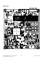
Page 37: ... 38 LGE Internal Use Only Copyright 2008 LG Electronics Inc All right reserved Only for training and service purposes MAIN TOP ...

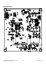
Page 38: ... 39 LGE Internal Use Only Copyright 2008 LG Electronics Inc All right reserved Only for training and service purposes MAIN BOTTOM ...

Page 39: ... 40 LGE Internal Use Only Copyright 2008 LG Electronics Inc All right reserved Only for training and service purposes Control B D BOTTOM Control B D TOP PREAMP B D BOTTOM PREAMP B D TOP ...

Page 40: ...April 2008 Printed in Korea P NO MFL42027603 ...

Reviews: