background image

- 13 -

LGE Internal Use Only

Copyright  © 

 LG Electronics. Inc. All rights reserved.

Only for training and service purposes

6.3. Option selection per country

6.3.1. Overview

(1)  Tool option selection is only done for models in Non-USA 

North America due to rating

(2)  Applied model : LA4AV/W Chassis is applied in USA 

6.3.2. Method

(1)  Press ADJ key on the Adj. R/C, then select Country Group 

Menu.

(2)  Depending  on  destination,  select  KR  or  US,  then  on  the 

lower Country option, select US, CA, MX. Selection is done 

using +, - KEY

7. GND and HI-POT Test

7.1. GND & HI-POT auto-check preparation

(1)  Check  the  POWER  CABLE  and  SIGNAL  CABE  insertion 

condition

7.2. GND & HI-POT auto-check

(1)  Pallet moves in the station. (POWER CORD / AV CORD is 

tightly inserted)

(2) Connect the AV JACK Tester.

(3) Controller (GWS103-4) on.

(4) GND Test (Auto) 

     - If Test is failed, Buzzer operates.

     -  If  Test  is  passed,  execute  next  process  (Hi-pot  test). 

(Remove A/V CORD from A/V JACK BOX)

(5) HI-POT test (Auto)

     - If Test is failed, Buzzer operates.

     -  If  Test  is  passed,  GOOD  Lamp  on  and  move  to  next 

process automatically

7.3. Checkpoint

(1) Test voltage

    - GND: 1.5KV/min at 100mA

    - SIGNAL: 3KV/min at 100mA

(2) TEST time: 1 second

(3) TEST POINT

    - GND Test =  POWER  CORD  GND  and  SIGNAL  CABLE 

GND.

    - Hi-pot Test = POWER CORD GND and LIVE & NEUTRAL.

(4) LEAKAGE CURRENT: At 0.5mArms

8. AUDIO output check

8.1. Audio input condition

(1) RF input: Mono, 1KHz sine wave signal, 100% Modulation

(2) CVBS, Component: 1KHz sine wave signal (0.4Vrms)

(3) RGB PC: 1KHz sine wave signal (0.7Vrms)

8.2. Specification

No

Item

Min

Typ Max

Unit

Remark

1

Audio practi-

cal max 

Output, L/R

(Distor-

tion=10% 

max Output)

9.0

10.0

12

W

Measure-

ment condi-

tion

EQ Off

AVL Off

Clear Voice 

Off

DRC opera-

tion under 

12W

(42LY series)

8.5

8.9

9.8

Vrms

4.5

5

6

W

22/28LY 

Series

6

6.4

6.7

Vrms

2

Speaker 

(8Ω Imped

-

ance)

10.0 14.0

W

(1)  Measure-

ment 

condition

   -  EQ/AVL/

Clear 

Voice: 

Off

32/42LY 

Series

5

7

W

22/28LY 

Series

▪Measurement condition:

(1) RF input: Mono, 1KHz sine wave signal, 100% Modulation

(2) CVBS, Component: 1KHz sine wave signal 0.4Vrms

(3) RGB PC: 1KHz sine wave signal 0.7Vrms

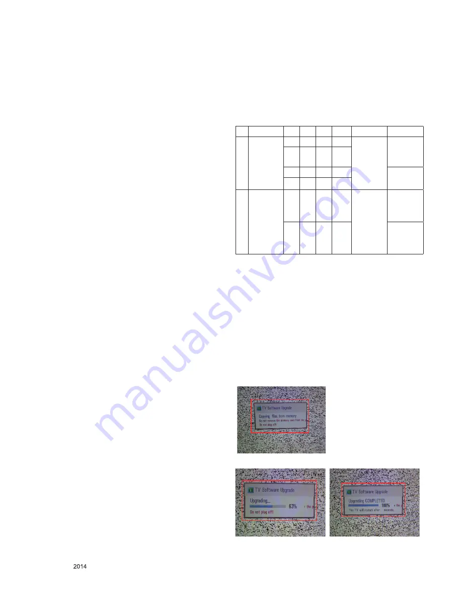
9. USB S/W Download 

    (optional, Service only)

(1) Put the USB Stick to the USB socket 

(2) Automatically detecting update file in USB Stick

  -  If your downloaded program version in USB Stick is lower 

than  that  of TV  set,  it  didn’t  work.  Otherwise  USB  data  is 

automatically detected.

(3) Show the message “Copying files from memory”

(4) Updating is staring.

Summary of Contents for 32LY560M

Page 1: ...ODEL 32LY560M 32LY560M UA CAUTION BEFORE SERVICING THE CHASSIS READ THE SAFETY PRECAUTIONS IN THIS MANUAL LED TV SERVICE MANUAL North Latin America http aic lgservice com Europe Africa http eic lgservice com Asia Oceania http biz lgservice com Internal Use Only ...

Page 2: ... LG Electronics Inc All rights reserved Only for training and service purposes CONTENTS CONTENTS 2 PRODUCT SAFETY 3 SPECIFICATION 4 ADJUSTMENT INSTRUCTION 8 TROUBLE SHOOTING 15 BLOCK DIAGRAM 19 EXPLODED VIEW 20 SCHEMATIC CIRCUIT DIAGRAM ...

Page 3: ...inals etc to be sure the set is safe to operate without damage of electrical shock Leakage Current Cold Check Antenna Cold Check With the instrument AC plug removed from AC source connect an electrical jumper across the two AC plug prongs Place the AC switch in the on position connect one lead of ohm meter to the AC plug prongs tied together and touch other ohm meter lead in turn to each exposed m...

Page 4: ...lectrostatic charge on your body by touching a known earth ground Alter natively obtain and wear a commercially available discharging wrist strap device which should be removed to prevent poten tial shock reasons prior to applying power to the unit under test 2 After removing an electrical assembly equipped with ES devices place the assembly on a conductive surface such as aluminum foil to prevent...

Page 5: ...he solder joints of the two original leads If they are not shiny reheat them and if necessary apply additional solder Fuse and Conventional Resistor Removal Replacement 1 Clip each fuse or resistor lead at top of the circuit board hollow stake 2 Securely crimp the leads of replacement component around notch at stake top 3 Solder the connections CAUTION Maintain original spacing between the replace...

Page 6: ...bout 5 minutes prior to the adjustment 3 Test method 1 Performance LGE TV test method followed 2 Demanded other specification Safety UL CSA IEC specification EMC FCC ICES IEC specification 4 General Specification No Item Specification Result Remark 1 Receiving System ATSC NTSC M 64 256 QAM 2 Available Channel 1 VHF 02 13 2 UHF 14 69 3 DTV 02 69 4 CATV 01 135 5 CADTV 01 135 3 Input Voltage AC 100 2...

Page 7: ...0 400 31 469 70 08 28 32 DOS O 3 640 480 31 469 59 94 25 17 VESA VGA O 4 800 600 37 879 60 31 40 00 VESA SVGA O 5 1024 768 48 363 60 00 60 00 VESA XGA O 6 1152 864 54 348 60 053 VESA X 7 1280 1024 63 981 60 020 108 0 VESA SXGA O 8 1360 768 47 712 60 015 85 50 VESA WXGA O 9 1920 1080 67 50 60 00 148 5 HDTV 1080P O HDMI DTV 1 720 480 31 500 60 000 27 027 SDTV 480P 2 720 480 31 470 59 940 27 000 SDTV...

Page 8: ...ard level and Final assembly adjustment items can be check using In Start Menu 1 Adjust Check Component 1080p and RGB PC Adjust will be calculated by 480i adjust value 3 2 Final assembly adjustment White Balance adjustment RS 232C functionality check Factory Option setting per destination Ship out mode setting In Stop 3 3 Appendix Ship out mode Service Option Default USB Download S W Update Option...

Page 9: ...successful ADC RGB Success is displayed and ADC RGB is completed If ADC calibration is failure ADC RGB Fail is displayed 3 If ADC calibration is failure after rechecking ADC pattern or condition retry calibration 5 2 EDID Download EDID PCM 5 2 1 Overview It is a VESA regulation A PC or a MNT will display an optimal resolution through information sharing without any necessity of user input It is a ...

Page 10: ...he one of R G B gain to 192 default data and decrease the others 3 Adj condition normal temperature Surrounding Temperature 25 5 ºC Warm up time About 5 Min Surrounding Humidity 20 80 Before White balance adjustment Keep power on status don t power off 6 1 1 2 Adj condition and cautionary items 1 Lighting condition in surrounding area surrounding lighting should be lower 10 lux Try to isolate adj ...

Page 11: ...192 G Gain j e 00 C0 192 B Gain j f 00 C0 172 R Cut 64 G Cut 64 B Cut 64 Applied Model 22LY560M UA Adj item Command lower case ASCII Data Range Hex Default Decimal CMD1 CMD2 MIN MAX Cool R Gain j g 00 C0 136 G Gain j h 00 C0 137 B Gain j i 00 C0 192 R Cut 64 G Cut 64 B Cut 64 Medium R Gain j a 00 C0 169 G Gain j b 00 C0 174 B Gain j c 00 C0 233 R Cut 64 G Cut 64 B Cut 64 Warm R Gain j d 00 C0 181 ...

Page 12: ...ked using no signal or Full white pattern 6 1 6 Reference White Balance Adj coordinate and color temperature Luminance 204 Gray 80IRE Standard color coordinate and temperature using CA 210 CH 14 Mode Coordinate Temp uv x y Cool 0 271 0 002 0 270 0 002 13000K 0 003 Medium 0 285 0 002 0 293 0 002 9300K 0 0000 Warm 0 313 0 002 0 329 0 002 6500K 0 0000 Standard color coordinate and temperature using C...

Page 13: ...min at 100mA SIGNAL 3KV min at 100mA 2 TEST time 1 second 3 TEST POINT GND Test POWER CORD GND and SIGNAL CABLE GND Hi pot Test POWER CORD GND and LIVE NEUTRAL 4 LEAKAGE CURRENT At 0 5mArms 8 AUDIO output check 8 1 Audio input condition 1 RF input Mono 1KHz sine wave signal 100 Modulation 2 CVBS Component 1KHz sine wave signal 0 4Vrms 3 RGB PC 1KHz sine wave signal 0 7Vrms 8 2 Specification No Ite...

Page 14: ...xternal Speaker Out 1 Connect external speaker to speaker out port with phone jack on TV rear bracket 2 Check the Max speaker output is 1W or not Sine wave with 1KHz will be displayed 3 Check Both of the signal in speaker only Power Fived 1W Default Check the input signal 1KHZ Sine wave and the waveform of output by utilizing oscilloscope 11 Pro Idiom 1 Connect RF cable 2 Press the Exit key for En...

Page 15: ...e Mstar IC101 or Main board Check Multi Voltage P401 9 10pin 24V 13 14 15pin 12V Replace Power Board Check DRV ON Control P401 2 pin High Check Power Board Check IC403 404 Q406 OutputVoltage IC403 1 1V IC404 1 5V Q406 3 3V Replace IC403 IC404 Q406 Re download software Check stand by Voltage L400 L401 3 5V Replace L400 L401 Check LVDS Power Voltage Q405 12V Replace Q405 Check Mstar LVDS Output Repl...

Page 16: ...ce L1600 Check IF_P N Signal TU1601 6 7 Pin Check Mstar LVDS Output Replace Mstar IC101 or Main Board ok ok ok No No No Bad Tuner Replace Tuner Check inputsignal format Is it supported Check AV Cable for damage for damage or open conductor Check JK1702 CVBS Signal Line R1722 ok ok ok No Replace Jack ok Check CVBS_DETSignal R1713 Replace R1713 No Check Mstar LVDS Output Replace Mstar IC101 or Main ...

Page 17: ...utput Replace Mstar IC101 or Main Board ok No Check inputsignal format Is it supported Check HDMICable conductors for damage or open conductor Check EDID Downlaod ok ok ok No Replace the defective IC or re download EDID data Check HDMISignal Check other set If no problem check signal line ok No Check Mstar LVDS Output Replace Mstar IC101 or Main Board ok No Replace Main Board No Check HDMI_DET HPD...

Page 18: ...damage Replace speaker ok No Off Toggle the Menu Check AMP IC IC5600 Power 24V 3 3V No Replace Amp IC IC5600 Check Output Signal P5600 1 2 3 4 pin No Check Mstar AUDIO_MASTER_CLK R123 No Replace Mstar IC101 or Main Board ok Check AMP I2C Line R111 R112 No Check signal line Or replace Mstar IC101 Replace Audio AMP IC IC501 Check signal line L5603 L5604 L5605 L5606 ok No Check RF Cable Signal Follow...

Page 19: ...U_CVBS X tal Reset IF_AGC SDA SCL_3 3V Reset Switch CS RE WE RX TX Micom MSP430F5419IPZR IC5002 24MHz JACK PACK at REAR SCL SDA_3 3V RF IC101 LGE2131 M1A_128M LAN S W Reset EXT_OUT I2C SCL SDA S_FLASH 8M bit MX25L8006EM2I 12G IC610 AUDIO AMP TPA3124D2PWPR IC1800 JK1800 JK5000 Pro Idom LGDT1001 IC1209 TS_CLK VALID SYNC 0 7 PM_TS_CLK VALID SYNC 0 7 TDJH H101F M P I HDMI 1 HDMI 2 RGB PC AV PC Audio U...

Page 20: ...lated characteristics These parts are identified by in the Schematic Diagram and EXPLODED VIEW It is essential that these special safety parts should be replaced with the same components as recommended in this manual to prevent X RADIATION Shock Fire or other Hazards Do not modify the original design without permission of manufacturer IMPORTANT SAFETY NOTICE 200 LV1 410 120 310 121 820 530 540 521...

Page 21: ...C104 2 AT24C256C SSHL T NVRAM_ATMEL EAN61133501 3 A2 2 A1 4 GND 1 A0 5 SDA 6 SCL 7 WP 8 VCC C105 0 1uF I2C_SDA IC104 3 BR24G256FJ 3 NVRAM_ROHM EAN62389502 3 A2 2 A1 4 GND 1 A0 5 SDA 6 SCL 7 WP 8 VCC R120 10K PDP IC104 M24256 BRMN6TP EAN61548301 NVRAM_ST 3 E2 2 E1 4 VSS 1 E0 5 SDA 6 SCL 7 WC 8 VCC R119 10K LCD PM_MODEL_OPT_0 PWM3 AMP_SCL R112 1K I2C_SCL I2C_SCL PWM_DIM IC104 1 R1EX24256BSAS0A NVRAM...

Page 22: ...ND_30 G15 GND_31 G16 GND_32 G17 GND_33 G18 GND_34 H7 GND_35 H8 GND_36 H9 GND_37 H10 GND_38 H11 GND_39 H12 GND_40 H13 GND_41 H14 GND_42 H15 GND_43 H16 GND_44 H17 GND_45 H18 GND_46 J7 GND_47 J8 GND_48 J9 GND_49 J10 GND_50 J11 GND_51 J12 GND_52 J13 GND_53 J14 GND_54 K8 GND_55 K10 GND_56 K11 GND_57 L10 GND_58 M5 GND_59 M7 GND_60 M8 GND_61 M9 GND_62 M10 GND_63 N4 GND_64 N5 GND_65 N6 GND_66 N7 GND_67 N8...

Page 23: ...R THE CRITICAL COMPONENTS IN THE SYMBOL MARK OF THE SCHEMETIC PCM_D 0 PCM_D 1 PCM_D 6 PCM_D 4 PCM_D 5 PCM_D 3 PCM_D 7 PCM_D 2 PCM_A 11 PCM_A 9 PCM_A 13 PCM_A 6 PCM_A 2 PCM_A 4 PCM_A 14 PCM_A 10 PCM_A 0 PCM_A 5 PCM_A 3 PCM_A 8 PCM_D 0 7 PCM_A 12 PCM_A 1 PCM_A 7 NON CI Region 3 2013 10 22 XXLY570H UA Non CI Region Copyright ⓒ 2014 LG Electronics Inc All right reserved Only for training and service p...

Page 24: ... OPT MHL_5V_EN 5V_USB C404 4700pF 50V 12V R459 0 OPT R409 10K R418 10 10uF C405 D401 30V MBR230LSFT1G 5V_Normal MHL_OCP_DET R408 4 7K C408 10uF 10V R403 4 7K OPT R410 100K TPS65282REGR IC400 1 EN 3 SS 7 FAULT2 9 SW_OUT2 10 RLIM 11 AGND 12 SW_OUT1 13 SW_IN_1 14 SW_IN_2 15 FB 16 LX_1 17 LX_2 18 BST 19 PGND_1 20 PGND_2 21 VIN_1 22 VIN_2 23 PGOOD 24 V7V 5 EN_SW2 8 FAULT1 6 EN_SW1 4 ROSC 2 COMP 25 EP G...

Page 25: ...6 7 8 9 C602 100pF 50V LED_R KEY2 IR R601 10K 1 C600 0 1uF 16V R602 3 3K 3 5V_ST R600 10K 1 R605 1 8K KEY1 3 5V_ST 3 5V_ST VA600 LED_R_Zener P601 12507WR 10L 1 2 3 4 5 6 7 8 9 10 11 C604 18pF 50V DIGITAL_EYE SENSOR_SCL SENSOR_SDA R604 1K DIGITAL_EYE C603 18pF 50V DIGITAL_EYE 3 3V_Normal R607 100 DIGITAL_EYE R606 100 DIGITAL_EYE R603 1K DIGITAL_EYE C605 0 1uF 16V C606 0 1uF 16V VA601 IR_Zener IR LE...

Page 26: ...TMDS_CH2 6 NC_1 7 NC_2 8 GND_2 9 NC_3 10 NC_4 D805 2 RCLAMP0524PA ESD_HDMI2_SEMTECH 1 8 2 7 3 6 4 5 9 10 D803 2 RCLAMP0524PA ESD_HDMI1_SEMTECH 1 8 2 7 3 6 4 5 9 10 D806 2 RCLAMP0524PA ESD_HDMI2_SEMTECH 1 8 2 7 3 6 4 5 9 10 D806 1 IP4283CZ10 TBA ESD_HDMI2_IP4283 3 GND_1 2 TMDS_CH1 4 TMDS_CH2 1 TMDS_CH1 5 TMDS_CH2 6 NC_1 7 NC_2 8 GND_2 9 NC_3 10 NC_4 R816 100 DDC_SDA_4 R827 10K VA807 OPT 5 6V D2 _HD...

Page 27: ...SB3157DFT2G EAN38256201 ANALOG SWITCH ON SEMICONDUCTOR 3 B0 2 GND 4 A 1 B1 6 SELECT 5 VCC IC1004 NLASB3157DFT2G EAN38256201 ANALOG SWITCH ON SEMICONDUCTOR 3 B0 2 GND 4 A 1 B1 6 SELECT 5 VCC 3 5V_ST R1008 100 IC1006 NLASB3157DFT2G EAN38256201 ANALOG SWITCH ON SEMICONDUCTOR 3 B0 2 GND 4 A 1 B1 6 SELECT 5 VCC 3 5V_ST UART3_RX S7_RX Update_SW S7_TX UART3_TX S7_TX S7_RX R1011 100 R1012 100 R1000 10K DE...

Page 28: ... HD 1 2 3 4 5 6 7 8 9 10 11 12 13 14 15 16 17 18 19 20 21 22 23 24 25 26 27 28 29 30 31 RXA1 RXA0 RXBCK RXA2 RXA2 RXA2 RXA2 Pol change RXBCK RXB4 LVDS_SEL RXB1 RXA3 RXB1 RXB3 RXACK RXBCK 30Pin LVDS Connector For HD 60Hz_Normal RXB3 RXA0 LVDS for large inch RXA3 RXA1 RXB0 RXA2 RXACK RXBCK RXACK RXA0 RXB2 RXB3 RXBCK RXACK RXA2 RXB4 RXB2 RXBCK RXA3 RXB2 RXA4 RXB2 RXB1 RXB2 Shift Change in S7LR RXA1 P...

Page 29: ... A MDQL7 A MDQL2 A MA0 A MA5 A MDQL3 A MA6 A MA10 C1206 0 1uF A MDQU1 A MBA2 C1221 1uF OPT A MDQSUB A MDQU7 A MCKB A MDQU5 1 5V_DDR A MDQL6 C1213 0 1uF A MDMU A MDML C1211 0 1uF A MCASB C1220 1uF OPT A MDQSL R1209 240 1 A MCASB A MDQU6 C1201 0 1uF C1212 0 1uF 1 5V_DDR A MDQL1 A MVREFCA A MA11 C1207 0 1uF C1219 1uF OPT A MA5 A MA14 1 5V_DDR A MA13 R1207 56 1 R1202 1K1 C1208 0 1uF C1203 10uF 10V A M...

Page 30: ...C 3 5V_ST C610 0 1uF IC610 MX25L8006EM2I 12G S_FLASH_MAIN_MACRONIX 3 WP 2 SO SIO1 4 GND 1 CS 5 SI SIO0 6 SCLK 7 HOLD 8 VCC SPI_CS R611 10K OPT R613 33 3 5V_ST IC610 1 W25Q80BVSSIG S_FLASH_MAIN_WINBOND 3 WP IO2 2 DO IO1 4 GND 1 CS 5 DI IO0 6 CLK 7 HOLD IO3 8 VCC FLASH_WP SPI_SDO SPI_SDI SPI_SCK 3 5V_ST R612 4 7K OPT Serial Flash 1MB 13 2013 08 17 XXLY670H UA S Flash Block Copyright ⓒ 2014 LG Electr...

Page 31: ...THE CRITICAL COMPONENTS IN THE SYMBOL MARK OF THE SCHEMETIC EPHY_RP VA1400 5 5V OPT VA1402 5 5V OPT EPHY_TN VA1401 5 5V OPT C1400 0 01uF 50V VA1403 5 5V OPT EPHY_TP EPHY_RN C1401 0 01uF 50V C1403 0 1uF 16V C1402 0 1uF 16V JK1400 RJ45VT 01SN002 1 2 3 4 5 6 7 8 9 9 ETHERNET 14 2014 01 21 32 42LY560M UA Ethernet Block Copyright ⓒ 2014 LG Electronics Inc All right reserved Only for training and servic...

Page 32: ... L503 2 10 0uH AMP_COIL_TAIYO R501 10K C511 0 1uF R507 470 24V_AMP SPK_L AMP_SCL C527 0 1uF 50V C522 330pF 50V L503 1 10 0uH AMP_COIL_GET C531 2200pF 50V OPT SPK_L C501 1000pF 50V C517 10uF 35V C505 0 047uF L503 AMP_COIL_ABCO 10uH C525 0 47uF 50V AMP_LC_0 47uF 24V_AMP L504 2 10 0uH AMP_COIL_TAIYO C508 4700pF L502 2 10 0uH AMP_COIL_TAIYO C534 2200pF 50V OPT R500 10K OPT AMP_RESET SPK_R AUD_LRCH C50...

Page 33: ...A OPT P1700 3AU04S 305 ZC LG 1 2 3 4 5 ZD1707 5V OPT SD05 C1717 5pF 50V OPT C1718 5pF 50V OPT R1716 10K VA1702 5 6V OPT R1721 1K 3 3V_Normal AV_CVBS_DET ZD1704 AV_CVBS_ZENER_ROHM C1710 47pF 50V ZD1703 1 AV_CVBS_ZENER_KEC ZD1704 1 AV_CVBS_ZENER_KEC ZD1703 AV_CVBS_ZENER_ROHM R1710 75 1 1608 AV_CVBS_IN R1715 10K C1708 1000pF 50V OPT R1714 10K AV_COMP_PC_R_IN C1709 1000pF 50V OPT AV_COMP_PC_L_IN VA170...

Page 34: ...SPK_CI R1814 100 EXT_SPK_NON_CI C1820 0 1uF 50V Ext_SPK_Switch R1817 27K Ext_SPK_Switch R1816 10K Ext_SPK_Switch C1824 3 3uF 50V Ext_SPK_Switch L1803 CPI2520NHL3R3ME Ext_SPK_Switch 2520 3 3uH Q1801 Ext_SPK_Switch MMBT3904 NXP E B C C1821 2 2uF Ext_SPK_Switch 50V Q1802 Ext_SPK_Switch_old AO3407A G D S R1818 22K Ext_SPK_Switch 24V EXT_SPK_DET External_SPK_VCC C1836 0 1uF 50V PILLOW_MUTE_INV 018 X12 ...

Page 35: ...20 AB7 C3013 0 1uF 16V 3 3V_Normal L3001 MLB 201209 0120P N2 R3018 220 BEXT_MPI_DOUT 020 AC7 Q3000 E B C 3 3V_TU D3010 5 6V OPT R3004 10K BEXT_IR_MODEM C3004 18pF 50V C3008 20pF 50V OPT R3007 82 OPT C3006 20pF 50V OPT TU_SIF IF_P_MSTAR C3003 18pF 50V TU_SDA TDJH H101F TU3000 47 SHIELD 6 IF P 7 IF N 8 NC_2 9 NC_3 1 B1 3 3V 2 NC_1 3 IF_AGC 4 SCL 5 SDA A1 A1 B1 B1 C3005 0 1uF 16V IF_AGC_MAIN C3000 0 ...

Page 36: ...N14 IO3_10 M13 IO3_11 M14 IO3_12 L13 IO3_13 M15 IO3_14 M16 IO3_15 L14 IO3_16 L15 IO3_17 L16 IO3_18 K16 IO3_19 K15 IO3_20 J16 IO3_21 H16 CLK3 G16 CLK2 H12 IO3_22 G14 IO3_23 G13 IO3_24 G15 IO3_25 F16 IO3_26 F14 IO3_27 F13 IO3_28 F15 IO3_29 E16 IO3_30 E15 IO3_31 D16 IO3_32 D15 IO3_33 F12 IO3_35 E13 IO3_36 H13 IO3_38 G12 IO3_39 B16 IO3_40 C15 IO3_41 C14 IO3_42 D13 IO3_43 B15 IO2_1 A15 IO2_2 B14 IO2_3 ...

Page 37: ... 2 A2 100 P6 3 A3 C5017 1uF C5008 2200pF Q5011 MMBT3904 NXP E B C Q5019 MMBT3904 NXP E B C Q5021 MMBT3904 NXP E B C Q5010 MMBT3906 NXP E B C C5025 47pF 50V OPT C5027 47pF 50V OPT SW5000 SKHMPWE010 1 2 4 3 5 SW5001 SKHMPWE010 1 2 4 3 5 C5004 0 1uF 50V C5013 0 1uF C5014 0 1uF C5015 0 1uF C5019 0 47uF CEC_REMOTE_PTC R5000 100 OPT PTC_TX R5002 330 C5020 0 1uF R5093 0 R5092 0 5V_ST 3 5V_ST_PTC R5128 10...

Page 38: ...W 1 C2301 10uF 16V R2329 3K Q2300 2SC3875S ALY E B C R2345 12K SEL_PILLOW_0 R2323 1 6K 1 4W JK2300 3 CH_UP 2 NC 1 ON OFF 6 CH_DN 5 AUDIO 4 COM 12VDC_1 023 AF4 C2306 0 1uF 50V R2304 3 6K 1 10W 5 R2317 10 1 4W 5 C2317 0 1uF 16V SEL_PILLOW_1 IC2300 MC34063ADR2G 3 TIMING_CAPACITOR 2 SWITCH_EMITTER 4 GND 1 SWITCH_COLLECTOR 5 COMPARATOR_INPUT 6 VCC 7 IPK_SENSE 8 DRIVER_COLLECTOR L2308 USP_1 R2337 470 1 ...

Page 39: ......

Reviews: