background image

- 19 -

LGE Internal Use Only

Copyright  © 

  LG Electronics. Inc. All rights reserved.

Only for training and service purposes

A2

A31

900

200

400

401

540

521

800

910

120

300

501

531

510

51

1

301

122

LV

1

801

571

570

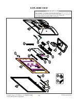
EXPLODED VIEW

Many electrical and mechanical parts in this chassis have special safety-related characteristics. These 

parts are identified by       in the Schematic Diagram and EXPLODED VIEW. 

It  is  essential  that  these  special  safety  parts  should  be  replaced  with  the  same  components  as 

recommended in this manual to prevent X-RADIATION, Shock, Fire, or other Hazards. 

Do not modify the original design without permission of manufacturer.

IMPORTANT SAFETY NOTICE

Summary of Contents for 26LN46 -Z Series

Page 1: ...P MODEL 26LN46 26LN46 Z CAUTION BEFORE SERVICING THE CHASSIS READ THE SAFETY PRECAUTIONS IN THIS MANUAL LED TV SERVICE MANUAL North Latin America http aic lgservice com Europe Africa http eic lgservice com Asia Oceania http biz lgservice com Internal Use Only ...

Page 2: ...nc All rights reserved Only for training and service purposes CONTENTS CONTENTS 2 SAFETY PRECAUTIONS 3 SERVICING PRECAUTIONS 4 SPECIFICATION 6 ADJUSTMENT INSTRUCTION 9 TROUBLE SHOOTING GUIDE 15 BLOCK DIAGRAM 18 EXPLODED VIEW 19 SCHEMATIC CIRCUIT DIAGRAM ...

Page 3: ...inals etc to be sure the set is safe to operate without damage of electrical shock Leakage Current Cold Check Antenna Cold Check With the instrument AC plug removed from AC source connect an electrical jumper across the two AC plug prongs Place the AC switch in the on position connect one lead of ohm meter to the AC plug prongs tied together and touch other ohm meter lead in turn to each exposed m...

Page 4: ...ctrostatic charge on your body by touching a known earth ground Alter natively obtain and wear a commercially available discharg ing wrist strap device which should be removed to prevent potential shock reasons prior to applying power to the unit under test 2 After removing an electrical assembly equipped with ES devices place the assembly on a conductive surface such as aluminum foil to prevent e...

Page 5: ...he solder joints of the two original leads If they are not shiny reheat them and if necessary apply additional solder Fuse and Conventional Resistor Removal Replacement 1 Clip each fuse or resistor lead at top of the circuit board hollow stake 2 Securely crimp the leads of replacement component around notch at stake top 3 Solder the connections CAUTION Maintain original spacing between the replace...

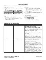
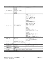
Page 6: ...rland Hungary Austria Slovenia Bulgaria France Spain Italy Belgium Russia Luxemburg Greece Czech Croatia Turkey Moroco Ire land Latvia Estonia Lithuania Poland Portugal Romania Albania Bosnia Serbia Slovakia Beralus DTV MPEG2 4 DVB T2 7 countries UK Sweden Denmark Finland Norway Ukraine Kaza khstan Ireland DTV MPEG2 4 DVB C 37 countries Germany Netherland Switzerland Hungary Austria Slovenia Bulga...

Page 7: ...3 3 4 5 6 256 QAM 1 2 2 5 2 3 3 4 5 6 DVB C Symbolrate 4 0Msymbols s to 7 2Msymbols s Modulation 16QAM 64 QAM 128 QAM and 256 QAM DVB S S2 symbolrate DVB S2 8PSK QPSK 2 45Msymbol s DVB S QPSK 2 45Msymbol s viterbi DVB S mode 1 2 2 3 3 4 5 6 7 8 DVB S2 mode 1 2 2 3 3 4 3 5 4 5 5 6 8 9 9 10 4 Scart 1EA PAL SECAM Scart jack is Full scart and support ATT DTV OUT not support DTV Auto AV 5 Video Input 1...

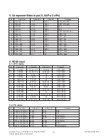
Page 8: ... Input 6 1 DTV mode No Resolution H freq kHz V freq kHz Proposed 1 640 480 31 469 31 5 59 94 60 SDTV 480P 2 720 480 31 469 31 5 59 94 60 SDTV 480P 3 720 576 31 25 50 SDTV 576P 4 720 576 15 625 50 SDTV 576I 5 1280 720 37 500 50 HDTV 720P 6 1280 720 44 96 45 59 94 60 HDTV 720P 7 1920 1080 33 72 33 75 59 94 60 HDTV 1080I 8 1920 1080 28 125 50 00 HDTV 1080I 9 1920 1080 26 97 27 23 97 24 HDTV 1080P 10 ...

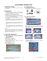
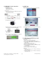
Page 9: ... C for 2 hours In case of keeping module is in the circumstance of below 20 C it should be placed in the circumstance of above 15 C for 3 hours Caution When still image is displayed for a period of 20 minutes or longer Especially where W B scale is strong Digital pattern 13ch and or Cross hatch pattern 09ch there can some afterimage in the black level area 3 Automatic Adjustment 3 1 MAC address D ...

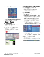
Page 10: ... menu 3 4 2 Method notice 1 Serial number D L is using of scan equipment 2 Setting of scan equipment operated by Manufacturing Technology Group 3 Serial number D L must be conformed when it is produced in production line because serial number D L is mandatory by D book 4 0 Manual Download Model Name and Serial Number If the TV set is downloaded by OTA or service man sometimes model name or serial ...

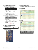
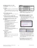
Page 11: ...ad NGx 3 5 2 Check the method of CI key value RS232 1 Into the main ass y mode RS232 aa 00 00 2 Check the mothed of CI key by command RS232 ci 00 20 3 Result value i 01 OK 1d1852d21c1ed5dcx 3 6 WIFI MAC ADDRESS CHECK 1 Using RS232 Command 2 Check the menu on in start 4 Manual Adjustment ADC adjustment is not needed because of OTP Auto ADC adjustment 4 1 EDID DATA 4 1 1 HDMI1 4 1 2 HDMI2 H freq kHz...

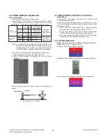
Page 12: ...rt Wheel key on the Adjustment remote control you can pairing with the TV SET 2 You can check the cursor on the TV Screen when select the Wheel key on the Adjustment remote control 3 You must remove the pairing with the TV Set by select Mute key on the Adjustment remote control 4 4 3D function test Pattern Generator MSHG 600 MSPG 6100 Support HDMI1 4 HDMI mode NO 872 pattern No 83 1 Please input 3...

Page 13: ...elect Network Connection option in Network Menu Step 3 Select Start Connection button in Network Connection Step 4 If the system finds any AP like blow PIC it is working well 4 7 LNB voltage and 22KHz tone check only for DVB S S2 model Test method 1 Set TV in Adj mode using POWER ON 2 Connect cable between satellite ANT and test JIG 3 Press Yellow key ETC SWAP in Adj Remote control to make LNB on ...

Page 14: ... 2 Checkpoint TEST voltage GND 1 5 KV min at 100 mA SIGNAL 3 KV min at 100 mA TEST time 1 second TEST POINT GND TEST POWER CORD GND SIGNAL CABLE METAL GND Internal Pressure TEST POWER CORD GND LIVE NEUTRAL LEAKAGE CURRENT At 0 5 mArms 5 Audio Measurement condition 1 RF input Mono 1 KHz sine wave signal 100 Modulation 2 CVBS Component 1 KHz sine wave signal 0 5 Vrms 3 RGB PC 1 KHz sine wave signal ...

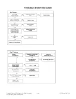
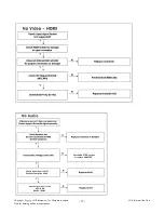
Page 15: ...G Electronics Inc All rights reserved Only for training and service purposes TROUBLE SHOOTING GUIDE IC2407 IC2407 P2400 PIN 12 Check backlight 24V P2400 1 5 Check STEP UP DC DC conv IC2406 P102 27 30 12V IC2408 12V output IC2408 P102 15 16 ...

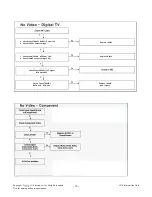
Page 16: ...g and service purposes 1 Check tuner TU6401 5 32 Power 3 3V 2 Check IC 2405 output voltage 1 Check tuner TU6401 7 Power 1 8V 2 Check IC6403 output voltage 1 8V Replace IC2405 Replace IC6403 Check Tuner TU6401 I2C signal 3 4 34 35 Check Tuner TU6406 DATA CLK SYN VAL Replace TU6406 And recheck ...

Page 17: ...Only Copyright LG Electronics Inc All rights reserved Only for training and service purposes Check signal from IC8101 P5400 output 1 2 3 4 Check ADAPTER output or replace ADAPTER Check signal from IC105 SCL SDA R5402 R5403 ...

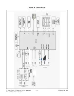
Page 18: ... 18 LGE Internal Use Only Copyright LG Electronics Inc All rights reserved Only for training and service purposes BLOCK DIAGRAM ...

Page 19: ...trical and mechanical parts in this chassis have special safety related characteristics These parts are identified by in the Schematic Diagram and EXPLODED VIEW It is essential that these special safety parts should be replaced with the same components as recommended in this manual to prevent X RADIATION Shock Fire or other Hazards Do not modify the original design without permission of manufactur...

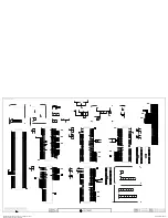
Page 20: ...30 H29 GPIO31 J26 GPIO32 G30 GPIO33 G27 GPIO34 E27 GPIO35 D29 GPIO36 D28 GPIO37 H28 GPIO38 J27 GPIO39 G29 GPIO40 G31 GPIO41 G28 GPIO42 B28 GPIO43 K28 GPIO44 E25 GPIO45 D21 GPIO46 G23 GPIO47 C28 GPIO48 F24 GPIO49 AB8 GPIO50 AA7 GPIO51 AD6 GPIO52 AC8 GPIO53 AC7 GPIO54 AB6 GPIO55 AC6 ADIN0_SRV AJ23 ADIN1_SRV AH23 ADIN2_SRV AE28 ADIN3_SRV AD28 ADIN4_SRV AF22 ADIN5_SRV AK21 ADIN6_SRV AG24 ADIN7_SRV AM1...

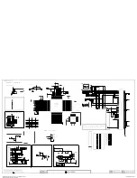
Page 21: ...705 1K 1 R702 1K 1 C712 0 1uF R703 1K 1 C710 0 1uF C711 0 1uF R711 240 1 R704 1K 1 H5TQ2G63BFR PBC IC702 DDR_256M_HYNIX A0 N3 A1 P7 A2 P3 A3 N2 A4 P8 A5 P2 A6 R8 A7 R2 A8 T8 A9 R3 A10 AP L7 A11 R7 A12 BC N7 A13 T3 A15 M7 BA0 M2 BA1 N8 BA2 M3 CK J7 CK K7 CKE K9 CS L2 ODT K1 RAS J3 CAS K3 WE L3 RESET T2 DQSL F3 DQSL G3 DQSU C7 DQSU B7 DML E7 DMU D3 DQL0 E3 DQL1 F7 DQL2 F2 DQL3 F8 DQL4 H3 DQL5 H8 DQL...

Page 22: ...G1FE3B B001 SAMSUNG_EMMC_4GB DAT0 A3 DAT1 A4 DAT2 A5 DAT3 B2 DAT4 B3 DAT5 B4 DAT6 B5 DAT7 B6 CLK M6 CMD M5 NC_3 A6 NC_4 A7 NC_23 C5 NC_42 E5 NC_43 E8 NC_44 E9 NC_45 E10 NC_52 F10 NC_58 G3 NC_59 G10 NC_66 H5 NC_73 J5 NC_80 K6 NC_81 K7 NC_82 K10 NC_116 P7 NC_119 P10 RSTN K5 VDD_1 C6 VDD_2 M4 VDD_3 N4 VDD_4 P3 VDD_5 P5 VDDF_1 E6 VDDF_2 F5 VDDF_3 J10 VDDF_4 K9 VDDI C2 VSS_2 E7 VSS_3 G5 VSS_4 H10 VSS_5...

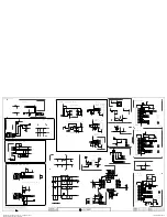
Page 23: ...pF 50V OPT C300 560pF 50V OPT C301 560pF 50V OPT R300 470K OPT C315 100pF 50V OPT Q3305 MMBT3904 NXP HDMI_EXT_EDID E B C C3300 0 1uF 16V OPT IC4303 BD82020FVJ 3 IN_2 2 IN_1 4 EN 1 GND 5 OC 6 OUT_1 7 OUT_2 8 OUT_3 R401 1K R400 470K VA400 5 6V L3302 BLM18PG121SN1D C3312 10uF 10V R3332 10K C3315 0 1uF 16V R3351 4 7K OPT R3306 4 7K HDMI_INTERNAL_EDID R3302 100 VA3309 ADLC 5S 02 015 VA3311 ADLC 5S 02 0...

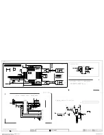
Page 24: ...NITOR_2 16 BST2B 17 PGND2B 18 OUT2B 19 PVDD2B 20 PVDD2A 21 OUT2A 22 PGND2A 23 BST2A 24 VDR2 25 AGND 26 VCC5 27 VDR1 28 BST1B 29 PGND1B 30 OUT1B 31 PVDD1B 32 PVDD1A 33 OUT1A 34 PGND1A 35 BST1A 36 RESET 37 AD 38 CLK_I 39 GND_IO 40 VDD_IO 41 EP GND L5404 LPH6045T 100M Audio_Coil_ABCO 10uH L5405 LPH6045T 100M Audio_Coil_ABCO 10uH L5402 LPH6045T 100M Audio_Coil_ABCO 10uH L5403 LPH6045T 100M Audio_Coil_...

Page 25: ...ET Q2406 MMBT3904 NXP E B C Q8800 MMBT3904 NXP E B C Q8811 MMBT3904 NXP E B C C2480 0 1uF 50V R2460 10 C2479 0 1uF 50V R2464 100K C2485 100pF 50V C2478 0 1uF 50V C2488 0 1uF 50V R2462 4 7K R2469 0 IC2408 NB634EL 3 SW_2 2 SW_1 4 SW_3 1 IN 6 BST 5 SW_4 7 EN SUNC 8 FB 9 PG 10 AAM 11 VCC 12 GND_1 13 GND_2 14 AGND 15 EP R2459 22K OPT R2463 82K L2412 15uH R2461 82K R2467 12K 1 R2466 820 1 R2465 33 1 R24...

Page 26: ... CI AR909 0 CI R907 47 CI C902 12pF 50V OPT R913 47K CI R908 47 CI R929 10K CI AR907 0 CI L4600 BLM18PG121SN1D EU VA4605 5 5V OPT VA4611 5 6V OPT R4601 10K EU L4601 BLM18PG121SN1D EU VA4604 5 5V OPT VA4608 5 6V OPT VA4601 5 6V OPT C4600 1000pF 50V EU C4601 1000pF 50V EU VA4610 5 5V OPT VA4603 5 5V OPT C4602 4700pF EU C4603 4700pF EU VA4607 5 6V OPT VA4606 5 6V OPT C4604 0 1uF EU VA4602 5 6V EU VA4...

Page 27: ...6V TU_W_BR TW CO JP R6509 33 R6513 10 TU_Q R6505 10K TU_N M_TW BR L6501 BLM18PG121SN1D TU_Q W C6521 0 1uF OPT C6520 0 1uF 16V TU_S N Q W C6500 18pF 50V TU_Q W_KR BR CO TW JP C6531 0 1uF C6538 10uF 10V C6542 0 1uF C6406 0 1uF 16V TU_N_BR R6411 0 TU_J_JP R6407 0 TU_J_JP R6405 0 TU_J_JP R6406 0 TU_J_JP R6409 0 TU_J_JP R6412 0 TU_J_JP R6410 0 TU_J_JP R6408 0 TU_J_JP C6602 0 1uF TU_M W R6602 100 TU_M W...

Page 28: ......
Reviews: