


29
ECP5 and ECP5-5G sysCLOCK
PLL/DLL Design and Usage Guide
PHASEDIR Input
The PHASEDIR input is used to specify which direction the dynamic phase shift will occur, advanced (leading) or
delayed (lagging). When PHASEDIR = 0 then the phase shift will be delayed. When PHASEDIR = 1 then the phase
shift will be advanced. The PHASEDIR signal must be stable for 5 ns before the PHASESTEP or PHASELOAD-
REG signals are pulsed. The PHASEDIR signal is optional and will be available if the user has selected the
Dynamic Phase ports option in Clarity Designer.
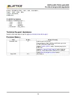
Table 16. PHASEDIR signal settings definition
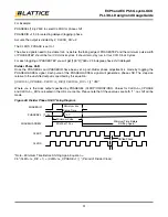
PHASESTEP Input
The PHASESTEP signal is used to initiate a
V
CO dynamic phase shift for the clock output port and in the direction
specified by the PHASESEL and PHASEDIR inputs. This phase adjustment is done by changing the phase of the
V
CO in 45
o
increments. The
V
CO phase changes on the negative edge of the PHASESTEP input after four
V
CO
cycles. This is an active low signal and the minimum pulse width (both high and low) of PHASESTEP pulse is four
cycles of
V
CO running period. The PHASESTEP signal is optional and will be available if the user has selected the
Dynamic Phase ports option in Clarity Designer. The PHASESEL and PHASEDIR are required to have a setup
time of 5 ns prior to PHASESTEP falling edge.
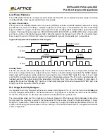
PHASELOADREG Input
The PHASELOADREG signal is used to initiate a post-divider dynamic phase shift, relative to the unshifted output,
for the clock output port and in the direction specified by the PHASESEL and PHASEDIR inputs. A phase shift is
started on the falling edge of the PHASELOADREG signal and there is a minimum pulse width of 10 ns from asser-
tion to deassertion. The PHASESEL and PHASEDIR are required to have a setup time of 5 ns prior to PHASEL-
OADREG falling edge.The PHASELOADREG signal is optional and will be available if the user has selected the
Dynamic Phase ports option in Clarity Designer.
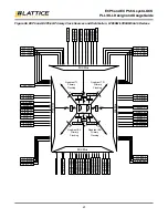
PLL Clock Outputs
The PLL has four outputs, listed in Table 17. All four outputs can be routed to the Primary clock routing of the
FPGA. All four outputs can be phase shifted statically or dynamically if external feedback on the clock is not used.
They can also statically or dynamically adjust their output duty cycle. The outputs can come from their output
divider or the reference clock input (PLL bypass). In bypass mode the output divider can be bypassed or used to
divide the reference clock.
Table 17. PLL Clock Outputs and ECLK Connectivity
PHASEDIR
Direction
0
Delayed (lagging)
1
Advanced (leading)
Clock Output Name
Edge Clock Connectivity
Selectable Output
CLKOP
Right, Left ECLKs
Always Enabled
CLKOS
Right, Left ECLKs
Selectable via Clarity Designer
CLKOS2
No ECLK Connection
Selectable via Clarity Designer
CLKOS3
No ECLK Connection
Selectable via Clarity Designer


