


5
iCE40 UltraLite Breakout Board
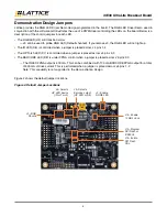
Clock Sources
The board has a single 12 MHz clock source. The 12 MHz clock drives both the FTDI USB interface device, and the
iCE40UL1K device. The iCE40UL1K device can be disconnected from the 12 MHz oscillator using J16. This is nec-
essary, for example, when iCE40 Ultra Lite device ball D2 is mistakenly programmed as an output and prevents the
FTDI USB interface from operating.
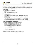
Board Power
The board provides the following power features:
• Board Power
— Board power is derived from the USB connection.
— D9 Green LED indicates Board Power
• iCE40 UltraLite VCC
— Onboard 1.2 V supply
— ICC can be measured across the series resistor R4 (1 Ohm) at test 1.2 V and VCC
• iCE40 UltraLite VCCIO
— Onboard 3.3 V supply
— ICC0 can be measured across the series resistor R2 (1Ohm) at test points TP4 and VCCIO0
— ICC1 can be measured across the series resistor R3 (1Ohm) at test points TP9 and VCCIO1
— ICC2 can be measured across the series resistor R5 (1Ohm) at test points TP6 and VCCIO2
Board Configuration and Programming
The board allows for programming of the iCE40 UltraLite or the SPI Flash:
• SPI Flash Programming J15 shunt pins 1-3 and 2-4 (Default shunted)
— U5 Micron Technology Inc part number N25Q032A13ESC40F
• iCE40 Ultra Configuration or Programming J15 shunt pins 1-2 and 3-4
— U1 iCE40UL1K-CM36A
• CRESETB can be asserted by pushing SW1
— Can be probed with J1
• DONE LED D2
— Can be probed with J2 (default shunted)
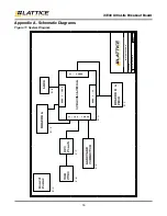
Details of the iCE40 UltraLite Board for use in programming are shown in Figure 3.


