


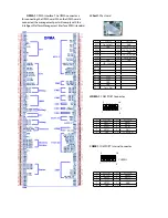


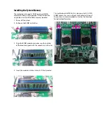


Motherboard Layout
The motherboard layout shows the connectors and
jumpers on the board. Refer to the following picture
as a reference of the pin assignments and the internal
connectors.
CFast1
COMB1
JDDR0-3
MGT1
JFAN2
JDDR12-15
CPU Socket
No.1
JVGA1
MGT2
JCOMA1
JOPMA1
J23
JFAN1
JFAN3 JFAN4
ATX3-4
ATX1-2
CPU Socket NO. 2
JLCM1
JUSB2
JUSB1
ATX5
CON3
SATA1-4
OPEN2
JOPEN1
JDDR4-11
J25
JSPIROM1
JTPM1
J80PORT1
JCMOS
J27
JGP1
JRISER1
JPCIESL4
JPCIESL3
JPCIESL2
JPCIESL1


